- id_12373661
- Version: 1.7
- Date: Dec 6, 2019 3:53:37 PM
Single Drive XRFD Amplifier Troubleshooting
Overview
The water-cooled, single drive XRFD RF amplifier is installed on some MR450w systems. The MR450w system originally had an air-cooled SRFD2 single drive RF amplifier. Newer systems have the water-cooled single drive XRFD RF amplifier.
The solid-state, water-cooled, single drive XRFD RF amplifier accepts a single RF input from an independent digital exciter (DTX1) unit to produce the single drive body and single drive head RF outputs. The DTX signal input at RF amplifier J14 provides the RF drive for the body RF output when the amplifier is in body mode. It also provides the head RF output when the amplifier is in head mode. A single unblank signal input at RF amplifier J20 is used to control the body and head output ports. The body output channel port is capable of 16 kW peak envelope power at 63.86 MHz, while the head port is capable of 2 kW peak envelope power at 63.86 MHz.
The amplifier has a single step digital rotary encoder used for RF gain adjustment. In body mode, it is used to adjust gain that controls body RF output. In head mode, it is used to adjust gain that controls head RF output. Due to the fact that it is a digital device it must only be adjusted when the amplifier is actively pulsing RF. Adjusting it when the amplifier is idle will have no effect later when the amplifier is actively pulsing RF.
In normal operation, the driver module provides a separate body and head TR bias signal to the RF amplifier. The amplifier couples the corresponding bias signal onto the body and head transmit outputs.
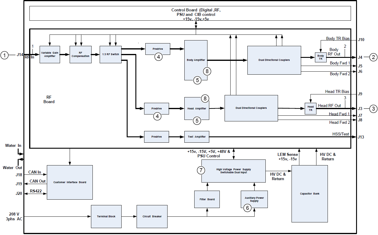
Similar to the 3T single drive XRFD, this unit is equipped with monitoring sensors located in key areas of the amplifier to aid with service activities.
| Callout on Functional Block Diagram | Connector Location | Sensor |
|---|---|---|
| 1 | J14 | RF In Exciter sensor |
| 2 | J4 | Body RF Out sensor |
| 3 | J3 | Head RF Out Sensor |
| 4 | None | Signal Conditioner Gain |
| 5 | None | Mode Gain |
| 6 | None | PSU1 and PSU2 Low Voltages |
| 7 | None | PSU1 and PSU2 High Voltages |
| 8 | None | Cold Plate Temperatures |
Figure 1. XRFD Amplifier Functional Block Diagram
The RF amplifier communication interface is based on the CAN open protocol. This provides enhanced transfer of information to the system. The CAN link provides communication to/from the amplifier from the scan control processor (SCP). The amplifier I/F (AIF) board provides unblank control, emergency shutdown, and a rudimentary secondary control link to the dual drive RF amplifier.
Diagnostic RF, voltage, and temperature sensors are located in various sections of the RF amplifier. Diagnostic tools gather data from these sensors during scanning. This data can then be used to help assess the condition of the head and body transmit circuits as well as the general health of the RF amplifier. The RF amplifier is designed to be a single replaceable FRU. This XRFD RF amplifier does not contain any replaceable internal FRUs.
For replacement information about the XRFD amplifier, see 1.5T RF Amplifier Replacement.
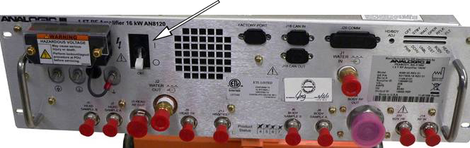
Connector Layout
The XRFD amplifier has connectors labeled specifically for body and head operation. There are also communication connectors, A/C power connectors, and two coolant connectors. For more details, see Figure 4.
See the table below for the connectors for body transmit on the XRFD amplifier.
Figure 2. Connectors for Body on XRFD Amplifier
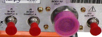
| Designator | Chassis Label | Description | Connector Type | Signal Type |
|---|---|---|---|---|
| J8 | BODY SAMPLE A | Body forward RF power sample | BNC female | Low level RF |
| J6 | BODY SAMPLE B | Body forward RF power sample | BNC female | Low level RF |
| J4 | BODY RF OUT | Body RF power out | 7/16 DIN female | High power RF with TR bias |
| J10 | BODY TR | Body TR bias input | BNC female | Switching DC control |
Connectors for Head
See the table below for the connectors for head on the XRFD amplifier.
Figure 3. Connectors for Head on XRFD Amplifier
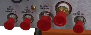
| Designator | Chassis Label | Description | Connector Type | Signal Type |
|---|---|---|---|---|
| J3 | HEAD RF OUT | Head RF power out | N female | High power RF with TR bias |
| J9 | HEAD TR | Head TR bias input | BNC female | Switching DC control |
| J7 | HEAD SAMPLE A | Head forward RF power sample | BNC female | Low level RF |
| J5 | HEAD SAMPLE B | Head forward RF power sample | BNC female | Low level RF |
Other Connectors
The illustration below shows J1, J2, J13, J14, J18, J19, and J20. The table below lists the connectors and their signal types.
Figure 4. Connectors on XRFD Amplifier
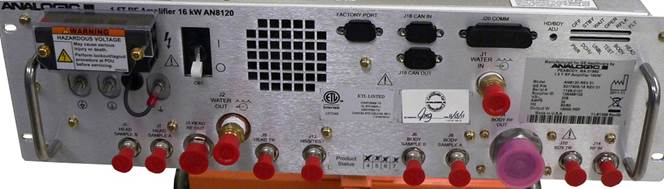
| Designator | Chassis Label | Description | Connector Type | Signal Type |
|---|---|---|---|---|
| J1 | WATER IN | Supply water | Male QD | N/A |
| J2 | WATER OUT | Return water | Male QD | N/A |
| J13 | HSS/TEST | RF (HSS) test port output | BNC female | Low level RF (400 mW ∓10%) (26 ∓ 0.4 dBm) |
| J14 | RF IN | RF input for Body and Head | BNC female | Low level RF (-4 to 4 dBm) |
| J18 | CAN IN | CAN communication (input) | 9-pin sub-D, female | Logic and 24 V |
| J19 | CAN OUT | CAN communication (output) | 9-pin sub-D, male | Logic and 24 V |
| J20 | COMM | General communication (input) | 25-pin sub-D, male | RS422 |
| N/A | FACTORY PORT | Unused | 9-pin sub-D, female | Unused |
AC Line Power Input Connector
The AC line power TB1 input connector is a terminal block supporting 3-phase power provided by the power distribution unit (PDU). These power connectors are located on the upper left portion of the XRFD amplifier. There are three incoming lines (L1, L2, and L3) and a ground connector.
Figure 5. TB1 Power Connector on XRFD Amplifier
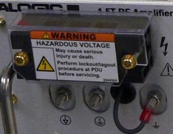
Circuit Breaker
The XRFD amplifier is protected by a circuit breaker.
Figure 6. Circuit Breaker on XRFD Amplifier
LED Indicators
The XRFD RF amplifier has two parallel banks of 6 LEDs.
The LEDs in the top bank (from right to left) are labeled FLT, RFLK, OPER, WAIT, STBY, and OFF.
The LEDs in the bottom bank (from right to left) are labeled HEAD, BODY, TEST, UNBL, DCHV, and PWR.
| Chassis Label | Color | Description |
|---|---|---|
| OFF | Yellow | Module in power off state. |
| STBY | Green | Module in standby state. |
| WAIT | Yellow | Module in transient, processing state. |
| OPER | Green | Module in operate state. |
| RFLK | Yellow | Module RFLOCK signal active. |
| FLT | Orange | Module in fault condition. |
| PWR | Green | Module AC power is on. |
| DCHV | Green | High voltage power supply active. |
| UNBL | Yellow | Unblank signal present. |
| TEST | Green | Module in test mode. |
| BODY | Green | Module in body mode. |
| HEAD | Green | Module in head mode. |
Troubleshooting Support
Diagnostic Capabilities
The XRFD amplifier contains several sensors that permit the monitoring of:
-
Internal PSU voltages
-
FET junction temperatures
-
Input and output peak and average RF power and VSWR for head and body RF output
These sensors are read by real-time system functions and diagnostic tools.
General Fault Isolation and Testing Process
Follow these general guidelines for troubleshooting XRFD amplifier issues:
-
From the Common Service Desktop, select Error Log > GE System Log to check for error messages regarding amplifier faults.
-
Read any extended error messages associated with the error fault (the error code number is highlighted in blue). Perform any recommended actions.
-
If necessary, execute one or more of the following tools or diagnostics:
-
For XRFD amplifier communication problems, run CAN Link Diagnostic to confirm communication of all devices on the CAN Link, including the XRFD amplifier.
-
For intermittent faults or those that only happen at a certain power level, run RF Power Check Tool .
-
For image quality problems due to the following:,
-
Poor RF stability or fidelity: Run the RF Analysis (RFA) tool. This tool permits testing and isolation to each component in the transmit chain.
-
Coherent Noise: Poor shielding inside the XRFD can result in coherent noise on the head transmit port. Refer to the Coherent Noise Troubleshooting procedure and search the PSDB for XRFD and Noise for the latest information.
-
-
To test the operation of the NB IF board in CAM and interconnection to XRFD amplifier, run RF Amp Interface Board Level Diagnostics.
-
Peripheral Hardware Reset
The system has a utility that allows you to start a hard-line reset to the amplifier if you think the microprocessors in the RF amp are locked up. This procedure is more aggressive than the CAN node reset executed by TPS. To access this utility from the Common Service Desktop, select the Utilities tab. In the Toolbox, select Peripheral Hardware Reset. Clear all check boxes except RF Amplifier Reset before running the utility.
Troubleshooting Hints
-
A poor RF load on the body or head RF transmit line can cause RF amplifier faults on a good, working RF amplifier. To prevent RF faults due to a bad RF load, connect the failing body or head RF output to a known good dummy load from the power measurement kit during testing. When using the 35kW dummy load, be sure to energize the dummy load fan.
-
The RF Amp Power Check Tool provides information about: output RF power, input RF power, unblank period, PSU voltage, and so on.
-
RF amplifier faults usually have an associated extended error message in the GE System Error log.
-
View XRFD PSU voltages in real time by typing mgd_term in a C-shell. Then in SCPWindow (at the prompt), type printVolts.
-
View XRFD PSU temperatures in real time by typing mgd_term in a C-shell. Then in SCPWindow (at the prompt), type printTemps.
-
View XRFD RF power in real time by typing Mgd_term in a C-shell. Then in SCPWindow (at the prompt), type printPower. The accuracy of the reported values depends heavily on the RF waveform in use and is inferior to that of the RF power measurement kit used during system calibration. Values reported by printPower are intended for troubleshooting purposes only. The RF waveform used by RF Amp Power Check Tool is designed to produce the best reported value results.