- id_12373514
- Version: 1.4
- Date: Dec 6, 2019 3:40:39 PM
CAM Theory and Troubleshooting
Identifying the CAM Chassis Configuration
The CAM chassis is supported in two different PGR cabinet configurations: one where there is a Cronus chassis present in the PGR cabinet and one where the Cronus chassis is absent.
| Cronus chassis is: | Gradient amplifiers are: | CAM chassis contains: |
| Present | XGA | SRF/TRF board |
| Absent | XG2 | PSE board |
Definition of Terms
- CAM chassis
-
Combined ASC and MGD chassis – combines the MGD and ASC functionality into one chassis. See MGD chassis or ASC chassis for the detailed board functionality. The differences between CAM chassis and MGD and ASC chassis are described in this document.
- ASC chassis
-
Amplifier Support Controller chassis – provides the narrow and broadband RF amplifier interface (control signals) and RF power monitoring. Boards in the ASC chassis remain on the CAN network. There is no direct bus communication between ASC and MGD components.
- MGD chassis
-
Multi-Generational Data acquisition chassis – consists of components that generate the timed control signals necessary to control the MR imaging system under the direction of the imaging sequence (pulse sequence). These control signals drive the gradient output and RF output, and gate the RF receive window. Details of the circuit board functionality is described below.
- Term server
-
In systems with the XGA configuration, the terminal server permits RS-232C serial connection to each of the processor boards (AGP, SCP, HEC) and the STIF board by using the existing Ethernet link.
In systems with the XG2 configuration, the terminal server permits RS-232C serial connection to each of the processor boards (AGP, SCP, HEC) and the PSE board by using the existing Ethernet link.
- Network switch
-
16- to 24-port gigabit Ethernet switch that provides a network path between the host computer and the ICNs, CAM processors, HEC, and term server. This network path is used for application download to the controllers, including downloading PSDs to the CAM. It is also used for serial communication between the host and the two CAM processor boards and the STIF board (XGA configuration) or PSE board (XG2 configuration).
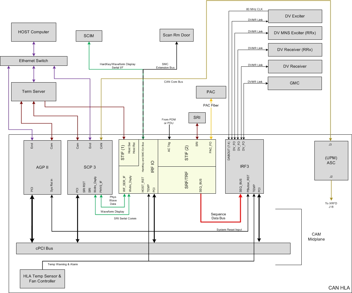
Block Diagram – Systems with XGA Gradient Amplifiers
XGA Gradient Amplifiers with STIF , SRF/TRF, and IRF3
XGA Gradient Amplifiers with PSE and IXG
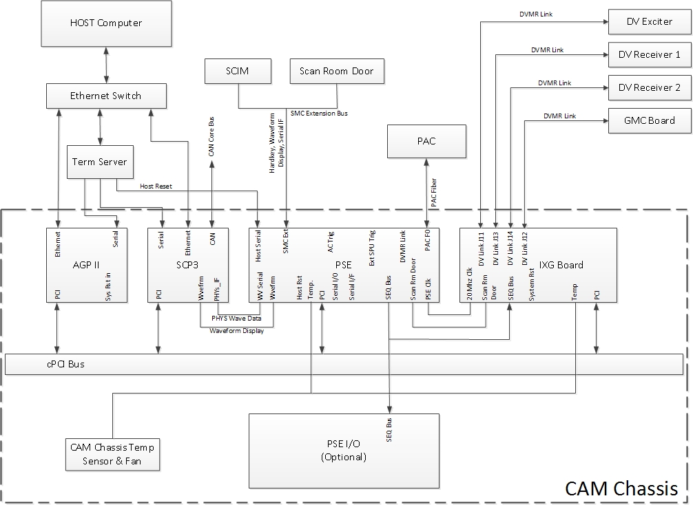
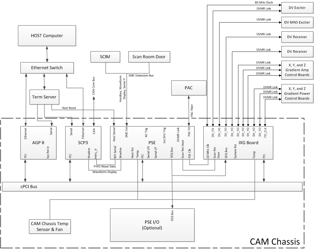
Block Diagram – Systems with XG2 Gradient Amplifiers
PGR Cabinet – Overview
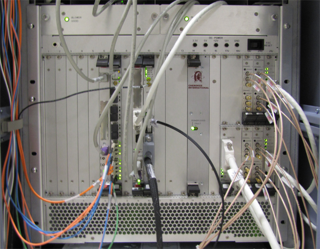
Figure 1. CAM Boards - Front View, System with XGA Gradient Amplifiers
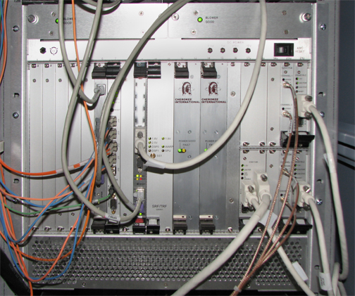
Figure 2. CAM Boards - Front View, System with XG2 Gradient Amplifiers
| Slot(s) Number | Board Name |
|---|---|
| From Left to Right | |
| 1-5 | Spare slots |
| 6 | AGP2 processor board |
| 7 |
(For systems with XGA configuration) IRF3 board (For systems with XG2 configuration) IXG board |
| 8 |
Spare slot |
| 9 | SCP3 board |
| 10–11 |
(For systems with XGA configuration) SRF/TRF board (For systems with XG2 configuration) PSE board (slot 10) and optional PSE I/O board (slot 11) |
| 12-13 |
Spare slot or power supply 2 note:
For the latest CAM chassis revisions, the second power supply (slots 12-13) is not necessary. |
| 14-15 | Power supply 1 |
| 16 | Spare slot |
| 17u-18u | Reserved for MNS IF board |
| 17L-18L | NB amplifier I/F board |
| 19u-19L |
Reserved for MNS detector board |
| 20u-20L |
NB amplifier detector board |
| 21u-21L | Processor board |
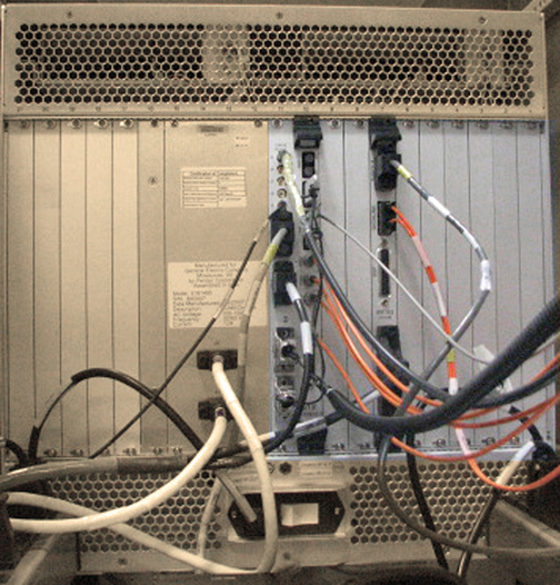
Figure 3. CAM Boards - Rear View, System with XGA Gradient Amplifiers
| Slot(s) Number | Board Name |
|---|---|
| 1-7 | Spare slots |
| 8 | IRF I/O |
| 9 | Spare slot |
| 10/11 | STIF |
In the XGA configuration, the CAM circuit boards are located on the front and the rear of the chassis. In the XG2 configuration, the CAM circuit boards are located on the front of the chassis, and all slots on the rear of the chassis are spare slots.
All boards connect to a common midplane and interface through a common compact PCI bus. Be careful when replacing or installing circuit boards in the CAM chassis, to avoid bending the small pins located on the midplane. Before installing or replacing a board into an empty slot, visually inspect the connectors on the midplane for bent pins. Also, check the female connector on the board for signs of damage before attempting to seat the board into the slot. The slots are keyed to prevent the insertion of an incompatible board.
The CAM is cooled by two fans located behind the metal cover plate at the top-front of the CAM chassis. The internal temperature of the CAM is monitored by two independent temperature sensors. Sensor 1 reports an over-temp condition when the temperature in the chassis reaches 40 °C (104 °F). Sensor 2 reports an over-temp condition when the temperature in the chassis reaches 50 °C (122 °F).
To load applications, the following boards must be installed in the CAM chassis: AGP board, SCP board, PS1. These boards must be installed in the correct slots with all the necessary cabling attached. If the software application fails to load or boot after software installation, and the CAM boards are installed and connected correctly, use “cu” (serial connection) or “rlogin” (Ethernet) to log in to each of the boards and monitor them for failures during TPS reset.
To remove the IRF, SRF/TRF, IRF I/O, STIF, IXG, and PSE boards: Retract the two screws that secure the boards to the CAM chassis, and press the inset gray tabs in to release the black chassis clips. Release the clips first to prevent damage.
Connectors on the IXG board are used as follows on a standard (non-MNS) system:
| Label | Function |
| J11 | Narrow band exciter |
| J12 |
(For XGA configuration) GMC board (For XG2 configuration) Not used |
| J13 | Receiver 1 |
| J14 | Receiver 2 |
| J15, J16, J17, J18, J19, J20 |
(For XGA configuration) Not used (For XG2 configuration) Connects to XPS2 X, Y, and Z and XGA2 X, Y, and Z |
| J8 | 80 MHz reference clock from exciter |
PGR Cabinet – CAM Chassis Front
AGP Board
The Application Gateway Processor (AGP) board provides an interface between the host application used to prescribe a sequence and real-time functions of the system that play out RF gradient waveforms prescribed by the sequence. The AGP provides two RJ45 connectors to interface with the host PC. The top connector provides an Ethernet link between the host and the AGP. During a TPS reset, data is transferred to the AGP via this link. The bottom connector provides a service RS-232 serial link between the AGP and the host via the term server.
Available diagnostics for testing the AGP board:
-
AGP and SCP Board Level Diagnostics: AGP
-
Host Datapaths: Ping > AGP
IRF3 Board (XGA Configuration)
The Interface and Remote Functions 3 (IRF3) board provides the interface between the system sequence control (SSC) subsystem (AGP and SRF/TRF) and the RF transmit subsystem (exciter), RF receive subsystem (receiver), and gradient subsystem (XGD). Refer to the following table for a description of the LEDs on the IRF3.
| Mnemonic | Function | Source |
| J10 RDY | Link-1 status | FPGA |
| J11 RDY | Link-2 status | FPGA |
| J12 RDY | Link-3 status | FPGA |
| J13 RDY | Link-4 status | FPGA |
| J14 RDY | Link-5 status | FPGA |
| RED OK | Reference clock detected | FPGA |
| PWR OK | Voltage OK | Voltage monitor |
| TRS REQ | System reset request | Push button |
The primary functions of the IRF3 board are:
-
To provide a communication interface between the IRF3 and the DTX, RRX, and XGD components via DVMR link.
-
To monitor the state of the DTX, RRX, and XGD subsystems to ensure they are functional.
Available diagnostics for testing the IRF3 board:
-
IRF3 Fiber Loop
-
IRF3 Wide Coverage
IXG Board
The IXG board is used only in the XG2 configuration.
The primary functions of the IXG board are:
-
80 MHz reference clock optical input
-
Synchronous synchronizer data transfer
-
Asynchronous PCI data transfer
-
Local capture of RRx header/footer/sample data
-
10 SFP optical transceiver modules with Digital Diagnostic Monitoring Interface (DDMI)
-
Scan room door interface
-
CAM clock distribution – 20MHz for PSE
-
20MHz sequence bus interface
-
CAM chassis temperature sensor monitoring
-
Front panel LED indicators
Available diagnostics for testing the IXG board:
-
IXG Board Level Diagnostics
-
PSE to IXG Datapath
| Mnemonic | Function | Functional Description |
| PWR OK | Power good | Turns green when power is applied to the board |
| REF OK | Reference clock OK | Turns green when the reference clock signal is detected |
| G_STAT | Master gradient status | Turns green when all axis controllers report ready and the gradient subsystem is in the ready state |
| HB | XGP NIOS heartbeat | Turns green when communication with XGP is active |
| J11 RDY | DVMR link interface link up | Turns green when DVMR link is active |
| J12 RDY | DVMR link interface link up | Turns green when DVMR link is active |
| J13 RDY | DVMR link interface link up | Turns green when DVMR link is active |
| J14 RDY | DVMR link interface link up | Turns green when DVMR link is active |
SCP Board
The Scan Control Processor (SCP) board controls the sequencing of the scan state. The SCP also provides an interface between the system sequence control (SSC) subsystem and the peripheral hardware in the patient handling subsystem. This interface is implemented over a CAN communication link to the scan room interface (SRI) board and allows the SSC subsystem to control and monitor the peripheral hardware, scan time display, and physiological interface.
The SCP provides two RJ45 connectors to interface directly with the host PC. The top connector provides an Ethernet link between the host and the SCP via the network switch. During a TPS reset, data is transferred to the SCP via this link. The bottom connector provides a service RS-232 serial link between the SCP and the host via the term server. The DB-9 connector provides the CAN port for the CAN communication link between the SCP and the SRI.
Available diagnostics for testing the SCP board:
-
AGP and SCP Board Level Diagnostics: SCP
-
SRI Datapaths: SRI SCP Loop Test, SRI STIF Loop Test (XGA configuration only)
-
CAM Datapaths: SCP > CAN
-
Host Datapath Diagnostics: Ping > SCP
SRF/TRF Board (XGA Configuration)
The Sequence Related Functions/Trigger and Rotational Functions (SRF/TRF) two-board assembly generates the RF and gradient waveforms. The SRF/TRF communicates with the RF subsystem through the IRF via cPCI backplane.
Two digital signal processors on the SRF board sequence the waveform data through the transformation processors and synchronize the waveform playout with the system hardware. The transformation processes are executed by the Waveform and Rotation Processor (WARP) and the Signal Processing Unit (SPU) on the TRF board. The WARP applies the gradient shim offsets, the oblique plane imaging rotation algorithm, and the frequency shifted B0 eddy current compensation (FRESBECC) algorithm to the waveforms prescribed in the PSD. The SPU on the TRF applies the gating algorithms to the sequences prescribed in the PSD.
Timing data for the gating algorithms is provided through a high speed serial interface to the physiological acquisition controller (PAC). This interface is also used by the TRF to monitor and display the physiological waveforms.
After a successful TPS reset, the DSP0, DSP1, and WARP LEDs will flash.
Available diagnostics for testing the SRF/TRF board:
-
CAM Board Level Diagnostics: TRF BLD, SRF BLD
-
CAM Datapaths: SRF > DRF, SRF > IRF, SRF > TRF
PSE Board
The PSE board is used only in the XG2 configuration.
The primary functions of the PSE board are:
-
Scan sequence playout
-
Digital pulse sequence waveform generation
-
Oblique plane image rotation
-
Real-time B0 eddy current compensation
-
Physiological gating algorithms
-
Physiological waveform display generation
-
Physiological acquisition controller (PAC) interface
-
Auxiliary physiological waveform interface
-
PC waveform/hardkey serial interface
-
Host serial interface
-
Trigger interfaces
Diagnostics available for the PSE board include PSE Board Level Diagnostics.
| LED | Name | Functional Description |
| DS1 | Host Reset | Indicates CPLD has detected a host reset event. Caused by either the host serial interface or the chassis reset push button. The LED remains on as long as either host reset source is active (host RX line held low, or push button held down) |
| DS2 | Power OK | On indicates all power rails are good |
| DS3 | SPU Heartbeat | Heartbeat LED indicating the SPU processor is running |
| DS4 | WARP Heartbeat | Heartbeat LED indicating the WARP processor is running |
| DS5 | NIOS Heartbeat | Heartbeat LED indicating the NIOS processor is running |
Power Supply Module
Early versions of the CAM chassis included two power supply modules. Later versions include only one power supply module. Both versions of the CAM chassis are equivalent.
The power supply module provides power to the CAM chassis. The output voltage this board provides cannot be adjusted. During normal operation the green Power Supply LED is illuminated. Some types of power supply failures cause the red Fault LED to illuminate. Test points next to each LED provide a convenient measurement location for checking the condition of each supply voltage with a digital multimeter.
ASC Reset Switch
The ASC reset switch, located at the upper right of the CAM chassis, resets the boards in the ASC section of the CAM chassis (slots 17 through 21). If there is a fault associated with the boards in these slots, pressing and releasing this switch may clear the fault.
PGR Cabinet – CAM Chassis Rear (XGA Configuration)
IRF I/O Board (Slot 11 R)
The Interface and Remote Functions Input/Output (IRF I/O) board provides a system monitor and control (SMC) interface by which the IRF3 board can monitor the scan room door status.
Available diagnostics for testing the IRF I/O board:
-
MGD Datapaths: IRF > IRF I/O
-
RRF Datapaths: RRF Loopback
STIF Board (Slots 13, 14 R)
The SRF/TRF Interface (STIF) board provides the fiber optic interfaces (fiber cables are not shown connected) for the fiber cables connecting to the PAC module inside the scan room. The coaxial cable connecting to J5 provides the 60Hz line clock signal from the AC distribution panel inside the cabinet. The gray cable equipped with the 9-pin sub-D connector provides an RS-232 serial link between the STIF board and the host via the term server. The function of this link is to supply the signal necessary to start a TPS reset when this is selected from the operator workstation. Physiological waveform data, physiological control data, and hardkey control data is transferred from connector J3.
Available diagnostics for testing the STIF board:
-
SRI Datapaths: SRI STIF Loopback
-
SRI Functional Tests: STIF - SRI Fiber Optic
-
Fiber Repeater Diagnostics: SRI STIF Loopback, SPU > STIF
PGR Cabinet – Term Server
(For XGA configuration) The term server is physically located next to the Ethernet switch. The term server permits RS-232C serial connection to each of the processor boards and the STIF board by using the existing Ethernet link. Serial ports are selected at the term server based on the information received in the Ethernet signal. The serial lines on the term server are connected as follows: port 1 connects to the HEC, port 2 connects to the AGP, port 3 connects to the SCP, and port 4 connects to the host serial reset port on the STIF board. Port 4 is required to complete a TPS reset from the host. The Ethernet cable from the term server can connect to any open port on the Ethernet switch.
(For XG2 configuration) The term server is physically located next to the Ethernet switch. The term server permits RS-232C serial connection to each of the processor boards and the PSE board by using the existing Ethernet link. Serial ports are selected at the term server based on the information received in the Ethernet signal. The serial lines on the term server are connected as follows: port 1 connects to the HEC, port 2 connects to the AGP, port 3 connects to the SCP, and port 4 connects to the host serial reset port on the PSE board. Except for the TPS reset that happens as part of a system reboot, port 4 is required to complete a manual TPS reset from the host. The Ethernet cable from the term server can connect to any open port on the Ethernet switch.
PGR Cabinet – Network Switch
The network switch is either a 16- or 24-port gigabit Ethernet switch. The status of each port is indicated by a set of LEDs on the front of the switch. The LEDs indicate link activity and link speed. Some models also show whether the communication is full or half duplex. In normal operation, each link with an Ethernet cable connected should show link activity and the Power LED should be lit/active. The Ethernet lines can be connected to any of the ports in any order. Connections can be swapped between any of the ports for troubleshooting.