- 00000018WIA30159F20GYZ
- id_131064691.31
- Jan 7, 2021 3:32:08 AM
ICE theory
Overview
The Integrated Control Engine (ICE) generates the signals that direct the Magnetic Resonance (MR) imaging system. ICE includes the ICE High Level Assembly (HLA) and ICE Mother Board (IMB). Some systems also include the ICE Daughter Board (IDB).
- ICE HLA
-
The ICE HLA consists of the IMB (and IDB, as applicable) that generates the timed control signals necessary to control the MR imaging system under the direction of the imaging sequence (pulse sequence). These control signals drive the gradient output and RF output, as well as gate the RF receive window.
- IMB
-
The IMB contains all of the base System Sequence and Control (SSC) functions. The IMB can operate with or without the IDB in a system requiring 32 (or fewer) channels.
- IDB
-
The IDB allows expansion of the imaging system up to 128 channels of receive data.
See ICE internal board for more information about the IDB and the IMB.
The following table explains ICE configurations for the applicable Optima systems.
| Marketing name | Magnet size | Table type | Software | Receive chain | SSC type | |||||
| Type | Channels | ICE | IDB | HLA part number | CAM | HLA part number | ||||
| Optima MR 450w GEM | 1.5T | GEM | DV25.1 or earlier | RRx | 32 | No | No | N/A | Yes | 5181495–8 or 5181495–61 |
| DV26.0 | RRx | 32 | Yes | No | 6200100-4 | No | N/A | |||
| DV29.1 or later | RRx | 32 | Yes | No | 6200100-110 | No | N/A | |||
| Note: Software upgrade from DV25.1 and earlier to DV26 do not require a hardware change. In these cases, these systems may still have CAM SSC. | ||||||||||
| 1. Discovery MR 450, Optima 450w BASE and Optima 450w GEM is no longer in forward production. | ||||||||||
| ICE HLA | HART log entry |
|---|---|
| 6200100-10: Support ≤160ch ICE Assembly: PSC, XGP, 4 REPs | 6250478 + 6250480 |
| 6200100-2: Support ≤128ch ICE Assembly: PSC, No_XGP, 3 REPs | 6250478-2 + 6250480-2 |
| 6200100-3: Support ≤32ch ICE Assembly: PSC, No_XGP, No_REPs | 6250478-2 |
| 6200100-4: Support ≤32ch ICE Assembly: PSC, XGP, No REPs | 6250478 |
| 6200100-5: Support ≤98ch ICE Assembly: 98CH, PSC, 66ch REPs | 6250478-3 |
| 6200100-110: Support ≤160ch ICE Assembly: PSC, XGP, 4 REPs | 6250478-10 + 6250480 |
| 6200100-102: Support ≤128ch ICE Assembly: PSC, No_XGP, 3 REPs | 6250478-12 + 6250480-2 |
| 6200100-103: Support ≤32ch ICE Assembly: PSC, No_XGP, No_REPs | 6250478-12 |
| 6200100-104: Support ≤32ch ICE Assembly: PSC, XGP, No REPs | 6250478-10 |
| 6200100-105: Support ≤98ch ICE Assembly: 98CH, PSC, 66ch REPs | 6250478-13 |
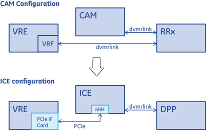
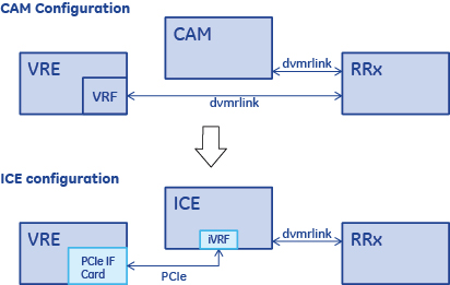
Platform changes from CAM to ICE
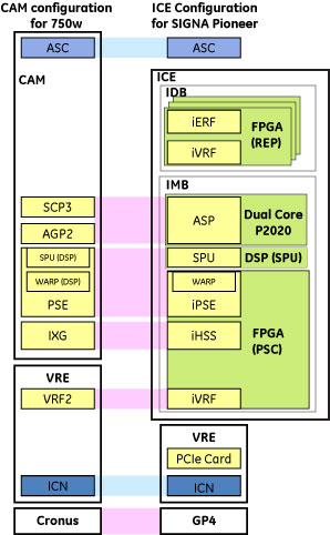
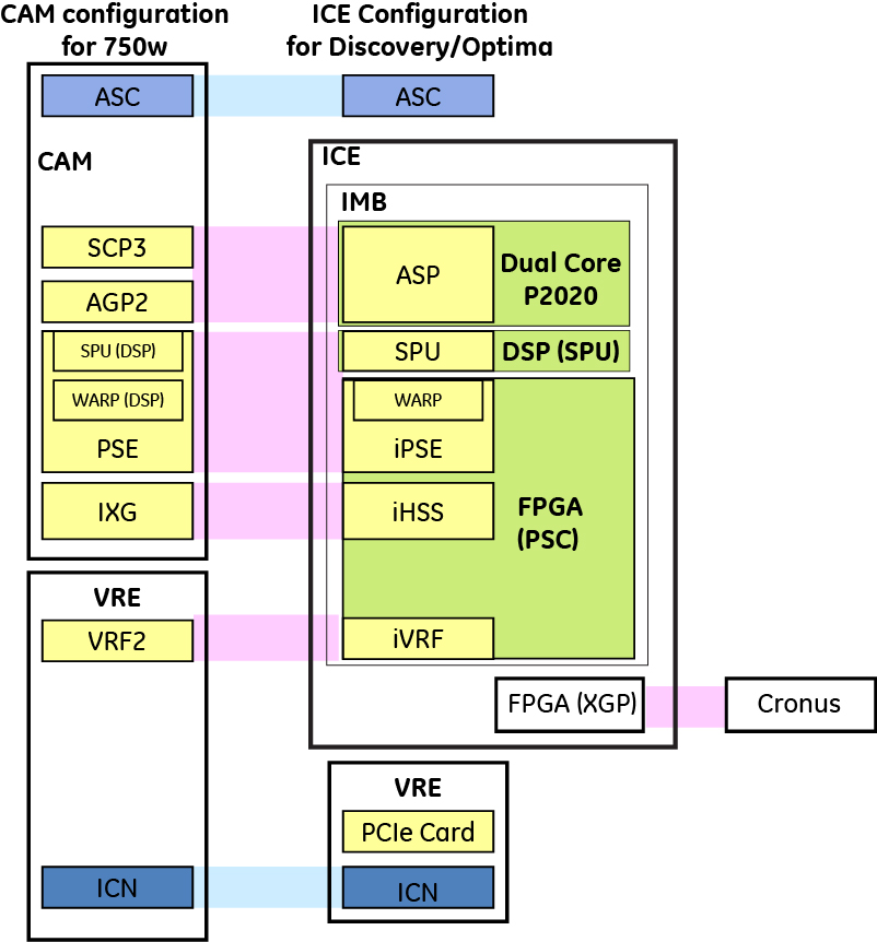
ICE mother board integrations
-
Real-time processor control: AGP and SCP processors collocated on a dual core P2020 Power PC processor.
-
System sequencing: All functions of the PSE board including WARP and SPU DSP functions. SPU function is implemented on the DSP, but all other functions are implemented in the PSC FPGA.
-
(For all Discovery, Optima, Signa Architect, Signa Artist, and Premier systems) System DVMRlink master: All IRF3-related functions are integrated into the PSC FPGA. XG2 control is consolidated into XGP.
-
Receive data filtering: Can filter 32 RF data channels (similar to VRF2 integrated into the PSC FPGA).
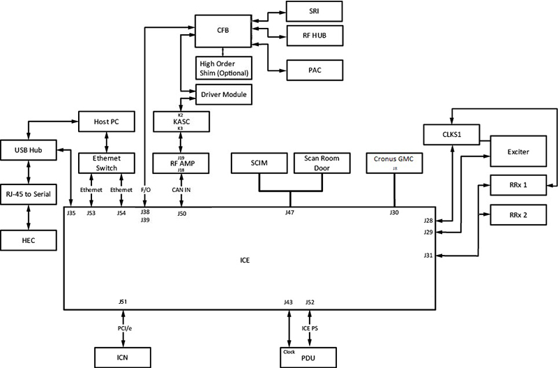
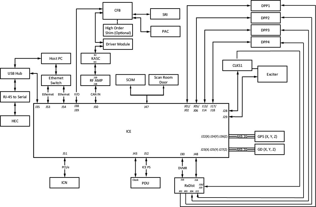
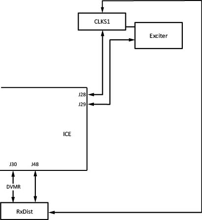
Block diagram
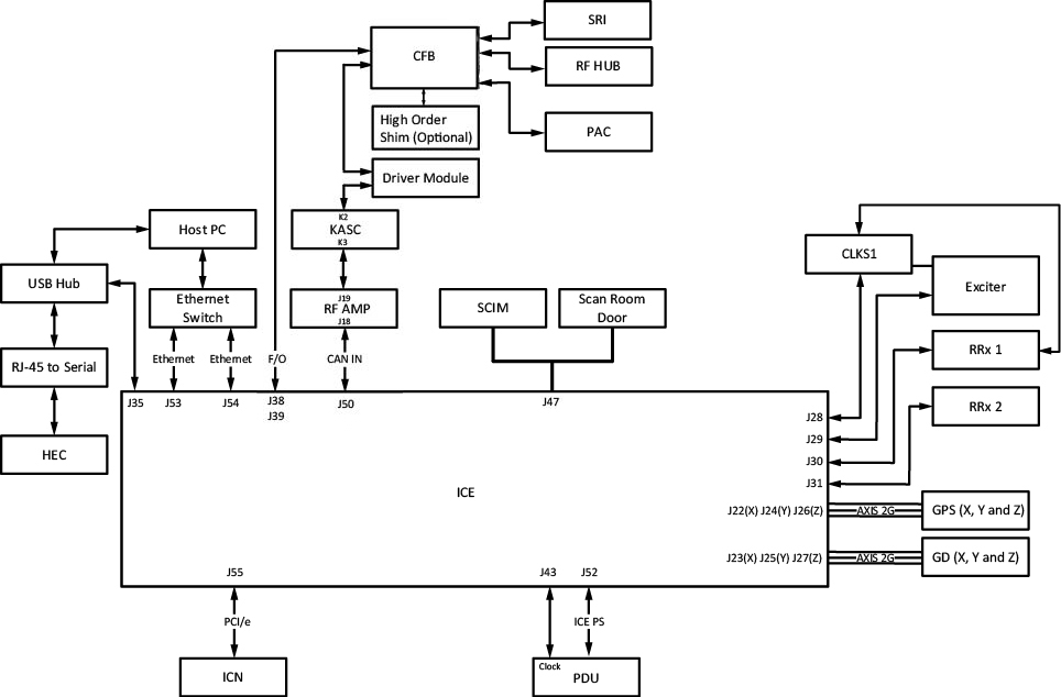
Cable connection
| Where (internal board) | J# (conn type) | Signal type | Connected to |
| Front (IMB) | J22 (SFP) | Axis 2G | GPS X |
| Front (IMB) | J23 (SFP) | Axis 2G | GD X |
| Front (IMB) | J24 (SFP) | Axis 2G | GPS Y |
| Front (IMB) | J25 (SFP) | Axis 2G | GD Y |
| Front (IMB) | J26 (SFP) | Axis 2G | GPS Z |
| Front (IMB) | J27 (SFP) | Axis 2G | GD Z |
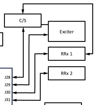
| Front (IMB) | J28 (TwinBNC) | System Clock | CLKS1 |
| Front (IMB) | J29 (SFP) | DVMRlink | Exciter |
| Front (IMB) | J30 (SFP) | DVMRlink | Rx Dist |
| Front (IMB) | J31 (SFP) | DVMRlink | RF Amp |
| Front (IMB) | J32 (SFP) | DVMRlink | N/C |
| Front (IMB) | J33 (DB15) | Engineering Use | N/C |
| Front (IMB) | J34 (DB15) | DABOUT | N/C |
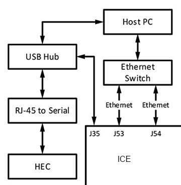
| Front (IMB) | J35 (USB) | USB | Host |
| Front (IMB) | J36 (SMB) | PSC Scope Trigger | N/C |
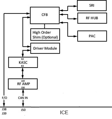
| Front (IMB) | J38/39 (LC) | PAC/SRI FO | CFB |
| Front (IMB) | J40/41 (LC) | No Connection | No Connection |
| Front (IMB) | J43 (BNC) | AC Trigger | Cab Mon |
| Front (IMB) | J44 (BNC) | External Trigger 1 | N/C |
| Front (IMB) | J45 (BNC) | External Trigger 2 | N/C |
| Front (IMB) | J47 (DB25) | SMC/PCHWK | Various |
| Front (IMB) | J48 (DB25) | Rx Chain Status | Rx Dist |
| Front (IMB) | J49 (DB9) | Aux Signal to SPU | N/C |
| Front (IMB) | J50 (DB9) | CAN | RF Amp |
| Rear (IMB) | J52 (7W2) | 48V DC Power | DC PS |
| Rear (IMB) | J53 (RJ45) | Ethernet | Hub |
| Rear (IMB) | J54 (RJ45) | Ethernet | Hub |
| Rear (IMB) | J55 (PCIe x4) | PCI express | ICN |
| Where (internal board) | J# (conn type) | Signal type | Connected to |
| Front (IMB) | J22 (SFP) | - | N/C |
| Front (IMB) | J23 (SFP) | - | N/C |
| Front (IMB) | J24 (SFP) | - | N/C |
| Front (IMB) | J25 (SFP) | - | N/C |
| Front (IMB) | J26 (SFP) | - | N/C |
| Front (IMB) | J27 (SFP) | - | N/C |
| Front (IMB) | J28 (TwinBNC) | System Clock | CLKS1 |
| Front (IMB) | J29 (SFP) | DVMRlink | Exciter |
| Front (IMB) | J30 (SFP) | DVMRlink | Cronus GMC J8 |
| Front (IMB) | J31 (SFP) | DVMRlink | RF Amp |
| Front (IMB) | J32 (SFP) | DVMRlink | N/C |
| Front (IMB) | J33 (DB15) | Engineering Use | N/C |
| Front (IMB) | J34 (DB15) | DABOUT | N/C |
| Front (IMB) | J35 (USB) | USB | Host |
| Rear (IMB) | J51 (PCIe x4) | PCI express | ICN |
| Rear (IMB) | J52 (7W2) | 48V DC Power | DC PS |
| Rear (IMB) | J53 (RJ45) | Ethernet | Hub |
| Rear (IMB) | J54 (RJ45) | Ethernet | Hub |
| Where (Internal Board) | J# (Conn Type) | Signal Type | Connected to |
| Front (IMB) | J01 (SFP) | DVMRlink | DPP1 |
| Front (IMB) | J02 (SFP) | DVMRlink | DPP1 |
| Front (IMB) | J05 (SFP) | DVMRlink | DPP2 |
| Front (IMB) | J06 (SFP) | DVMRlink | DPP2 |
| Front (IMB) | J13 (SFP) | DVMRlink | DPP3 |
| Front (IMB) | J14 (SFP) | DVMRlink | DPP3 |
| Front (IDB) | J17 (SFP) | DVMRlink | DPP4 |
| Front (IDB) | J18 (SFP) | DVMRlink | DPP4 |
| Front (IMB) | J22 (SFP) | Axis 2G | GPS X |
| Front (IMB) | J23 (SFP) | Axis 2G | GD X |
| Front (IMB) | J24 (SFP) | Axis 2G | GPS Y |
| Front (IMB) | J25 (SFP) | Axis 2G | GD Y |
| Front (IMB) | J26 (SFP) | Axis 2G | GPS Z |
| Front (IMB) | J27 (SFP) | Axis 2G | GD Z |
| Front (IMB) | J28 (TwinBNC) | System Clock | CLKS1 |
| Front (IMB) | J29 (SFP) | DVMRlink | Exciter |
| Front (IMB) | J30 (SFP) | DVMRlink | Rx Dist |
| Front (IMB) | J33 (DB15) | DABOUT | N/C |
| Front (IMB) | J34 (DB15) | Engineering Use | N/C |
| Front (IMB) | J35 (USB) | USB | Host |
| Front (IMB) | J36 (SMB) | PSC Scope Trigger | N/C |
| Front (IMB) | J38/39 (LC) | PAC FO | CFB J7/J8 |
| Front (IMB) | J43 (BNC) | AC Trigger | Cab Mon |
| Front (IMB) | J44 (BNC) | External Trigger 1 | N/C |
| Front (IMB) | J45 (BNC) | External Trigger 2 | N/C |
| Front (IMB) | J47 (DB25) | SMC/PCHWK | Various |
| Front (IMB) | J48 (DB25) | Rx Chain Status | Rx Dist |
| Front (IMB) | J49 (DB9) | Aux Signal to SPU | N/C |
| Front (IMB) | J50 (DB9) | CAN | RF Amp |
| Rear (IMB) | J51 (PCIe x4) | PCI express | ICN |
| Rear (IMB) | J52 (7W2) | PCI express | DC PS |
| Rear (IMB) | J53 (RJ45) | Ethernet | Hub |
| Rear (IMB) | J54 (RJ45) | Ethernet | Hub |
Key connection features
PCIe communication
The PCI communicates between the VRE and the ICE.
An IXH610 PCIe interface card (dolphin card) with updating EEPROM is used in the VRE.
-
VRF function moves to the ICE PSC FPGA from the VRE in CAM configuration.
-
(For Signa Architect, Artist, Pioneer, Voyager, and Premier systems) PCIe cable should connect to IDB PCIe connector instead of IMB.
-
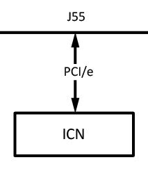
(For Discovery, Optima, SIGNA Creator / Explorer, SIGNA MR355 / MR360 systems) PCIe cable should connect to PCIe connector J55.
- (For Discovery and Optima systems with XGD gradients) PCIe cable should connect to PCIe connector J51.
USB extender
-
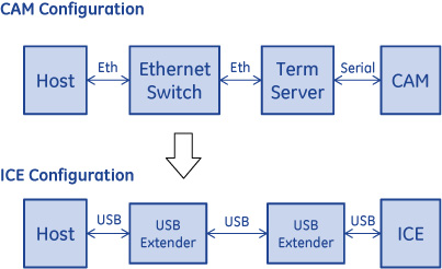
Direct USB Connection instead of Ethernet + Term Server.
-
USB-Serial conversion on IMB.
-
USB repeater boards exist on both the ICE & Host sides
-
New Host-CPLD interface via USB.
CAN connection
Copper CAN connection:
-
(For Pioneer and Voyager systems) Copper CAN:
-
(For Signa Architect, Artist, Discovery, and Optima systems) Copper CAN:
Fiber CAN connection:
-
(For Signa Architect, Artist, Pioneer, and Voyager systems) Fiber CAN: SRI4
-
(For Discovery and Optima systems)
Clock distribution
-
Copper twin BNC clock connection instead of optical connector for enhanced reliability.
-
Note: Forward production Architect and Artist systems eliminate the clock splitter.
-
CLKS1 splits 80MHz clock from the Exciter to the ICE and receive chain.
ICE behavior at 80MHz clock loss
The ICE module resets itself when the 80MHz external clock to ICE J28 is lost. At the time of reset the following error messages are logged in gesyslog:
-
(For 2223892) The system has reported a reference clock error. This may be a result of the E-stop button being pressed.->
-
(For 2261910) The previous reset of the ICE module was caused by a loss of the external REF clock. The ICE module will reset itself if this clock fails. PSC->
-
(For Discovery, Optima, Signa Architect, Signa Artist, and Premier systems) If a scanning session is open at the time of external clock loss, the following message appears in the FSA status bar area.
Figure 17. ICE error 
-
TPS reset is required in order to recover the system. During TPS reset, the ICE re-confirms whether the external clock is present or not. If it is still missing, the ICE module forces TPS reset to fail. At this failure, either one of the following two messages are logged in gesyslog, depending on the situation.
Case 1
2261925 The ICE module does not have an external RefClk but the RxDist module does. No DVMR fiber links will function.->
[Suspected Root Cause] CLKS1 (J3 side), ICE, Clock line between CLKS1 J3 and ICE J28.
Case 2
2261924 The ICE module and the RxDist module do not have an external REF clock. No DVMR fiber links will function.->
[Suspected Root Cause] Exciter module power (DCPS), Exciter (clock source), CLKS1 (J1 side), clock line between Exciter and CLKS1 J1.
Case 3
No message is logged in this case. In some system types, E-stop disconnection can cause REF clock loss.
-
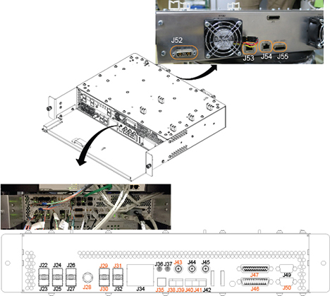
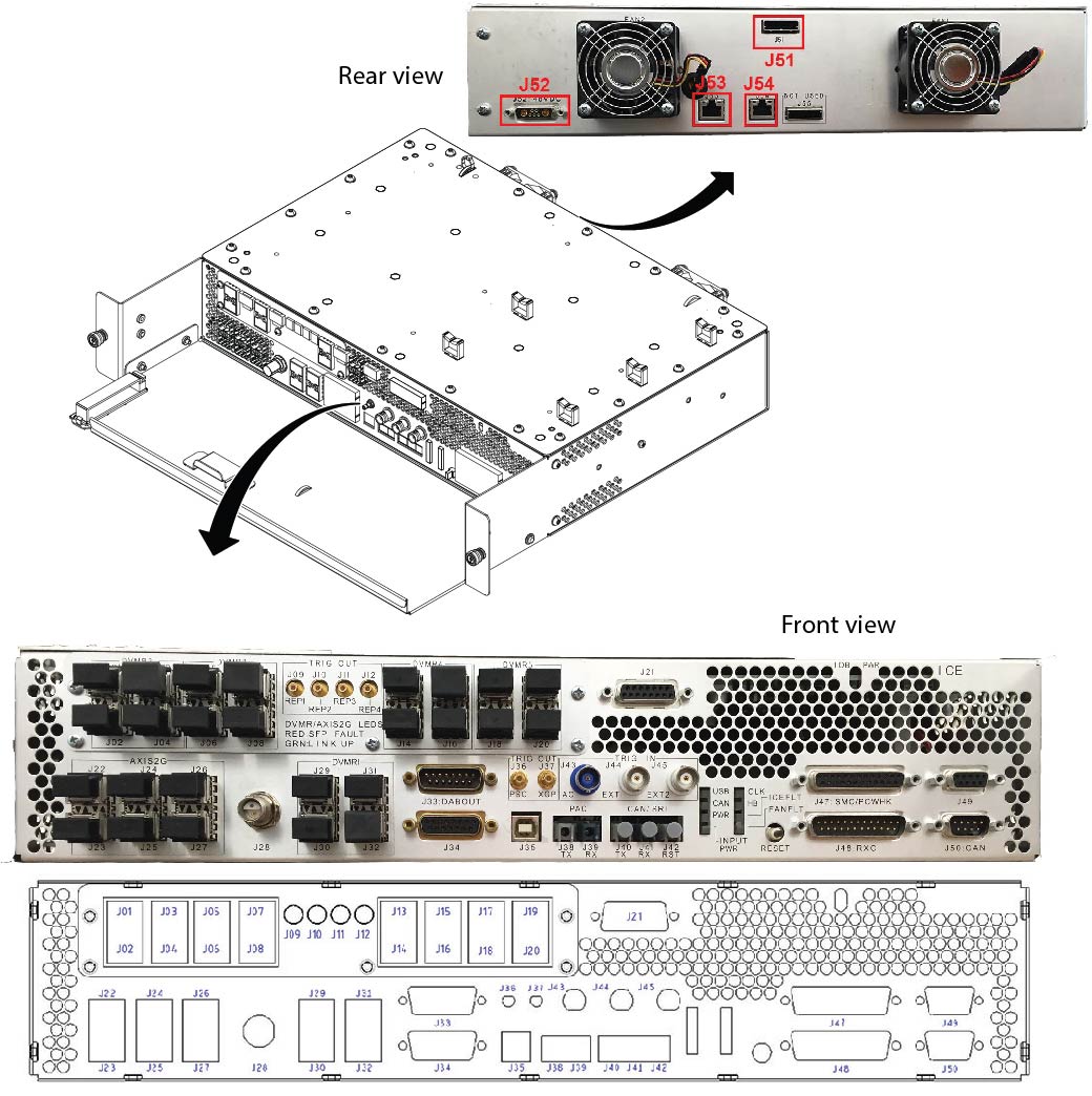
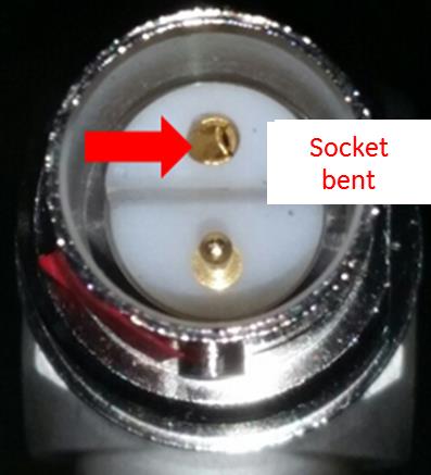
Twin BNC connector (J28) for 80 MHz clock
The Twin BNC connector has to be correctly aligned before mating. The internal sockets may be bent as shown in illustration below or the pin of the cable connector may be bent if the cable connector is just pushed to J28 and twisted to find the correct position. Note that the cable and connector must be visually aligned before attempting to seat the connector.
DVMR link
| Warning | |
|---|---|
| Notice | |
|---|---|
| Notice | |
|---|---|
(For Signa Architect, Artist, Pioneer, Voyager, and Premier systems) The RF analog signal from the MR coils is converted into a digital signal in the DPP (digitized per pin) and the digital data is sent to the iVRF within the ICE chassis thorough DVMRlink. See Receive Chain Theory for more information.
(For Discovery and Optima systems) The RF analog signal from the MR coils is sent to the iVRF within the ICE Chassis thorough DVMRlink. See Receive Chain Theory for more information.
LEDs
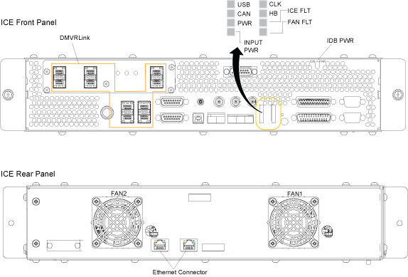
| Mnemonic | Functional description |
| USB POWER | This green LED will turn on when USB power is detected. This LED will turn on when USB power is present – even if ICE input power is removed. This LED being off may indicate that the host is off or that there is a problem with the USB cable running between the host and the ICE. |
| CAN | This green LED will blink when traffic is present on the copper CAN interface (J49). |
| CLK |
This green LED indicates the status of the ICE reference clock (J28).
|
| HB | This green LED acts as a heartbeat LED driven by the AGP SCP Processor (ASP) on ICE:
|
| ICE FLT | ICE fault: Software will turn this red LED on if an error occurs during Power-On Self Test (POST). The LED will also be held on when ICE is in reset. This LED will normally be off. |
| FAN FLT | Fan fault: Software will turn the red LED on if a problem is detected with one (or both) of the fans on the rear of the ICE assembly. Check the system error log to identify which of the two fans has failed. The ICE fans are FRUs and can be replaced independently of the full ICE assembly. The LED will also be held on when the ICE is in reset. This LED will normally be off. |
| INPUT PWR | This green LED indicates ICE input power is present. ICE receives 48VDC via J52 on the rear side of the enclosure. If this LED is off, ICE input voltage is low or missing. Check the power source and cabling to find the root cause. It is possible that this LED may be off (or dim) in a low voltage situation while the ICE unit itself remains functional as the circuit that drives this LED is configured to turn the LED off before the internal power supplies reach a fault condition. |
| PWR | This green LED will turn on when the ICE motherboard internal power supply voltages are present. This LED being off indicates an internal power fault on the ICE motherboard. If this LED is off – first verify ICE input power is present (INPUT PWR LED and error log). If input power is ok, power cycle the ICE and replace the unit if the internal power fault doesn’t clear. |
| Green DVMRlink LEDs | LED on: The corresponding link is up. LED off: The corresponding link is down. |
| Red DVMRlink LEDs | LED on: The corresponding SFP is either missing or has reported a fault and should be replaced. The SFP is a FRU. LED off: The corresponding SFP is present and not reporting a fault. |
Each Ethernet connector on the back of the ICE assembly (J53 and J54) contains two externally visible LEDs.
| Mnemonic | Functional description |
| Green LED: Link 1000/Activity |
|
| Yellow LED: Link/Activity |
|
Under normal operating conditions, both Ethernet links should train to 1000BASE-T mode so both green and yellow LEDs should be on and blinking with traffic. If just the yellow LED is on/blinking, or both LEDs are off, then there may be a problem with that Ethernet link.
ICE internal board
ICE Mother Board (IMB)
The IMB is one of two boards that may exist in the ICE High Level Assembly (HLA). The IMB contains all of the base SSC functions and can operate with or without a daughter board in a system that requires 32 (or fewer) receive channels and up to two parallel transmit channels. The ICE Daughter Board (IDB) allows expansion of this system up to 128 receive channels and eight parallel transmit channels. See ICE daughter board (IDB) for more information about the IDB.
IMB features:
-
P2020 Dual Core PowerPC with real-time VxWorks OS.
-
High-speed PCIe replaced cPCI backplane.
-
USB-to-serial on board for host communication.
-
Sequencer, DVMRlink comm., VRF in one PSC FPGA
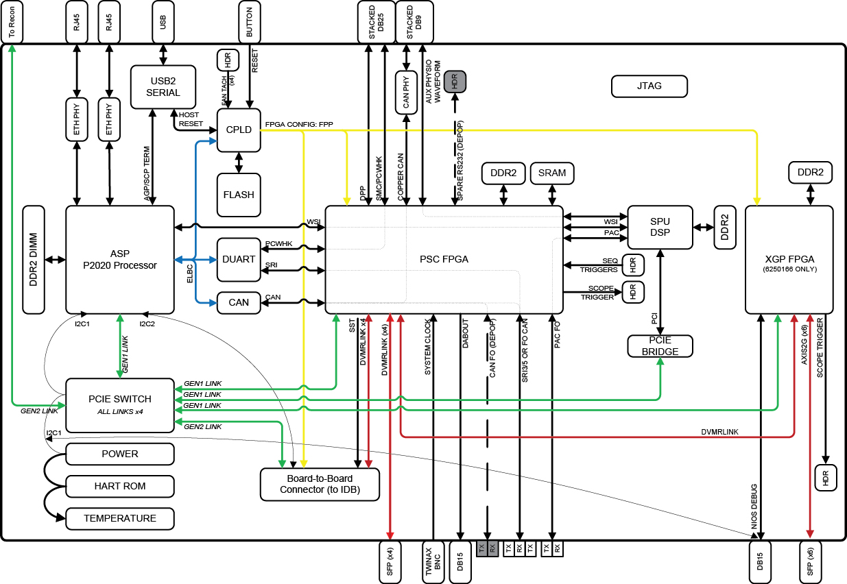
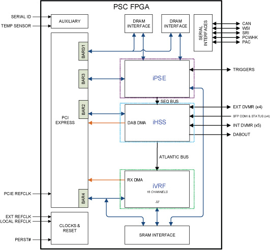
PSC FPGA
-
iPSE
-
Sequence processor: Accesses DDR2 SDRAM to construct SSP/RF/Grad waveform data.
-
WARP: Applies rotation matrix for oblique scan, eddy current compensation for B0, B0 drift compensation.
-
SEU (sync exec unit): Synchronize sequence data playout on sequence bus with trigger and 4us tick.
-
-
iHSS
-
Interfaces with four external and five internal DVMRlinks.
-
(For DPP receive chain systems) Delay module exists to establish synchronized DVMRlink communication from the IMB and IDB.
-
(For RRx receive chain systems) Delay module exists to establish synchronized DVMRlink communication from the IMB.
-
FDM as new function for data validity check which replaces monitor fifo in iPSE.
-
-
iVRF
-
Decimation filter for received data from the receive chain.
-
R2 digital gain adjustment.
-
Two 16 channel-supported modules.
-
Filtered data DMA transfer to recon via PCIe.
-
ICE daughter board (IDB)
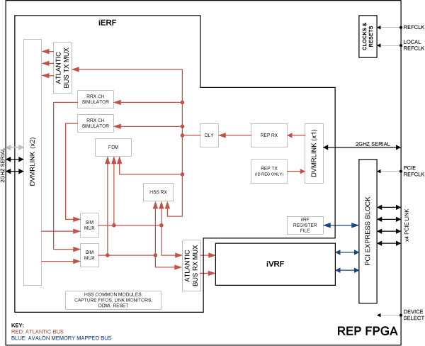
Three identical REP FPGAs reside in the ICE daughter board, which supports the signal receive capability up to 96 channels and can generate up to six unique channels of RF data. When combined with the mother board, the ICE HLA can support 128 receive channels and generate eight unique RF data channels. Each FPGA has the DVMRlink communication with the PSC FPGA, which resides in the ICE mother board, and three external DVMRlink communications with remote devices.
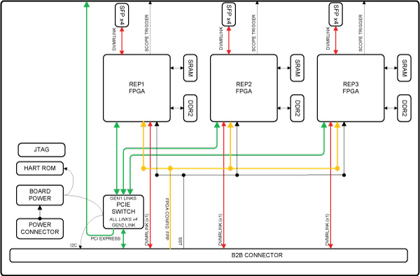
The internal logic of the REP FPGA can be divided into two main functional blocks: iERF and iVRF.
-
iERF
-
Expand DVMRlink communication with one DPP (up to 32 channels).
-
FDM (same function as in PSC FPGA).
-
-
iVRF (completely identical to iVRF in PSC FPGA)
-
Decimation filter for received data from receive chain.
-
R2 digital gain adjustment.
-
Two 16 channel-supported modules.
-
Filtered data DMA transfer to recon via PCIe
-