- Topic ID: id_17423005
- Version: 3.0
- Date: Apr 22, 2019 12:56:00 AM
CDAS Theory
1 Overview
The CDAS (Chiclet base Data Acquisition System) is a new architecture DAS system based on the new generation ASIC. Based on current CDAS and Merc40 architecture, many ASIC control and data processing are moved to VCS, CDAS function is more simplified compared with previous DAS product. The function of the CDAS is included but not limited:
-
Provide power and control signals to the Detector VCS modules.
-
Provide diagnostic capability for the CDAS and Merc40 Detector.
-
Format and package raw data from VCS, then transmit view data out to system via the slip ring communications hardware
CDAS consists of three types of boards, 1pcs CDCB, 1pcs PB and 1pcs BP, as well as the necessary mechanics to provide thermal, electromagnetic compatibility (EMC) and structural support for the electronics.
2 Block Diagram
Figure 1. CDAS Block Diagram
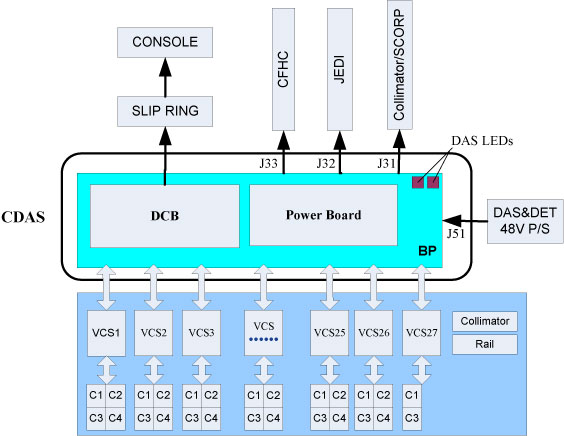
This diagram shows the CDAS architecture and relationship with other sub-system.
3 Function of each board
3.1 CDCB
3.1.1 Processing
There is one CDCB for DAS & Merc40 detector control and external system communications interface which includes data and commands. CDCB has the below functions:
-
Based on LVDS serial communication physical layer, generates clocks, LS, and HS for 27pcs VCS, also a single end Reset signal.
-
Programs the VCS Modules’ operating mode through the GXL protocol between CDAS and VCS of Merc40 Detector.
-
Sets up scan frequency, arm_scan registers to VCS through LS signals between CDAS and VCS of Merc40 Detector.
-
Collects and de-serializes the data from 27pcs VCS through HS signals between CDAS and VCS of Merc40 Detector.
-
Incorporates Forward Error Correction in the data and sends it across the slip ring interface to the DAS Interface processor (DIP).
-
Transmits the data across the RF slip ring serially on a high-speed, 2.488 Gbps fiber-optic link which consists of two optical fibers to the slip ring.
-
Detects jitter and timeouts in the view trigger signal.
-
Performs analog to Digital conversion of auxiliary channels for Power supply on CDCB. Performs analog to Digital conversion for kV and mA from the generator.
-
Control of the DAS operation modes is done by the SCORP via a 1Mbit/sec capable Controller Area Network (CAN) interface, known as the Rotating Controller Interface Bus (RCIB). The RCIB also supplies a CAN Fault line and FLASH download.
-
Sends configuration and set up commands to the Detector Common Fan and Heater Control (CFHC) Board via an RS232 link and monitors the thermal subsystem for faults.
-
Sums the Z-Axis reference channels internally, and communicates with the collimator to allow tracking of the x-ray beam in the Z-axis.
-
Diagnoses DAS faults using feedback and built in tests.
-
Supports scanning at trigger rates up to 2811 Hz.
-
Voltage Monitoring
Below is block diagram of CDCB.
Figure 2. CDCB Block Diagram
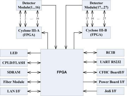
CDCB will get 3.3V, ±12V voltage from PB and then create its own internal voltages less than 3.3V.
3.1.2 LED’s
Below are the test points and LED's available on the DCB.
3.2 PB (Power Board)
There is one PB in CDAS design. This Power Board’s main functions are:
-
Provide the 3.3V and +/-12V power to CDCB.
-
Provide the 3.3V and 1.8V power to VCS module.
-
VCS power ON-OFF control.
-
Provide DC-DC module status by LEDs.
Below are block diagram of PB.
Figure 3. Power Board Block Diagram
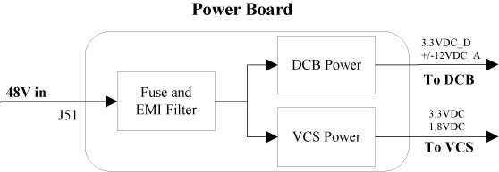
Test Point and LED’s
Below are the test points and LED's available on PB.
3.3 BP (Back Plane)
There is one backplane in CDAS design. BP is not only interconnection between CDAS and Merc40 detector, but also external connection between CDAS and SCORP, JEDI, CFHC and 48V power supply. The optical cables attach directly to the CDCB without BP.
The backplanes:
-
Convey the power from PB to the Merc40 Detector VCS boards, from PB to CDCB
-
Act as an interface between the Merc40 Detector VCS digital cables and the CDCB to transfer the Digital data and control signals. This interface is still called the DDIF (DAS Detector Interface) although it is now a Digital interface compared to the analog interface between the detector and DAS in past products.
-
Provide connectors for interfacing the CDCB CAN bus communications to/from the Rotating Controller Interface Bus (CT-RCIB), the CDCB with the detector Common Fan and Heater Controller(CFHC), and the generator kV and mA signals.
-
There’ re another two CDAS status LEDs on BP. One is Heart_LED and another is Error_LED.
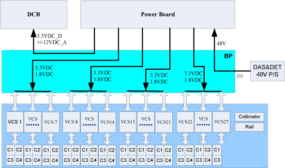
4 Power Line
The following shows the Power Line Wiring Diagram.
Figure 4. Power Line Wiring Diagram
5 Power Supply
The 48V power supply is a single power supply on the rotating assembly that powers the DAS, Detector subsystem, Collimator, ORP, Heater/Fan control board and Slipring Transmitter.
The Power supply has an internal fan for cooling.
6 External Interface
CDAS has five major external interfaces:
6.1 Merc40 Detector VCS Boards
-
Power for the VCS module, 3.3V and 1.8V.
-
20MHz Clocks for command and data transmission
-
200MHz LS signals to setup and control for VCS boards.
-
600MHz HS signals to handle data from the Detector to CDAS.
6.2 CFHC
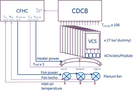
Detector thermal control is via the CFHC on the back of detector plate. CDAS DCB sends the module temperature to CFHC and get the feedback from CFHC including fan info, heater info, and detector module temperature status.
Figure 5. Gantry Rotating Side Thermal Block Diagram
6.3 Generator
CDAS measures scan kV and mA from the X-ray Generation Subsystem, then insert kV and mA digital values into the view data stream. The Generator Interface is implemented on a connector located on BP and signals are routed to CDCB via the backplane. Here is a description of the KV and MA signals coming from the generator.
-
kV feedback in differential analog form
-
mA feedback in differential analog form
6.4 Collimator and SCORP via the RCIB (Rotating Controller Interface Bus)
-
System Control messages via CAN
-
Serial data from SCORP
-
Triggers
-
RCIB CAN fault assertion
-
RCIB reset
-
Power for the CAN
6.5 Slip Ring
-
Two, 2.488 GHz optical data links.
-
FEC for data integrity.
-
Data randomizing for EMI reduction