- Topic ID: id_17423431
- Version: 2.0
- Date: Dec 21, 2018 2:36:14 AM
HDAS with SDCB Theory
1 Overview
New Optima CT660 DAS subsystem is designed to improve the cost performance from HDAS_Saturn_64 (HDAS with 64 slice Saturn detector) by using SuperDCB (SDCB) board. The cost saving is done by DIFB reduction. The HDAS with SDCB has 4 slave blocks which consist of DSP and FPGA, instead of 15 DIFBs at HDAS. The HDAS with SDCB is compatible with the 64 slice HALO Detector. This section explains the differences between conventional HDAS_Saturn_64 DAS system and HDAS with SDCB System. Please refer to VDAS and HDAS Theory for not explained functions in this section.
2 Block Diagram
Figure 1. HDAS_Saturn_64 Block Diagram
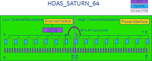
Figure 2. HDAS with SDCB Block Diagram
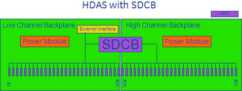
In case of HDAS_SATURN_64, AD Module output is connected to DIFB board and DIFB sends the data to DCB. 4 AD Module is connected to one DIFB. In case of SDCB, all of AD modules are connected to SDCB and the data is sent from AD Module to SDCB directly. And there is no signal cable between Back planes, it’s done by SDCB inside.
3 HDAS with SDCB (SuperDCB)
3.1 Introduction
The function of the HDAS with SDCB is to
-
Provide power and control to the Detector AD modules
-
Provide diagnostic capability for the DAS and Detector
-
Format and linearize the data, and transmit it out to system via the slip ring communications hardware
It consists of three types of boards, SDCB (Das Control Board), two Power Modules and two backplanes (Low channel and High channel) as well as the necessary mechanics to provide thermal, electromagnetic compatibility (EMC) and structural support for the electronics. The DAS will be capable of providing data and scanning at 2811 Hz trigger rate.
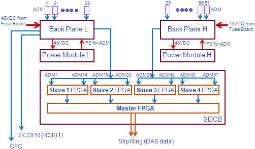
Figure 3. HDAS with SDCB Detail Block Diagram
3.2 Function of each board
3.2.1 SDCB
SDCB consists of Master block and Slave block. Master block is equivalent to DCB, and Slave block is equivalent to DIFB.
Master block has the following functions:
-
Programs the Detector Analog Modules’ operating mode through the Slave block. Set up the gain and offset trim for the Slave blocks via the Internal CAN. Provides a Reset signal for the Slave blocks and the Analog Modules.
-
Collects and de-serializes the data from the slave block, checksums and formats the data for view transmission.
-
Incorporates Forward Error Correction (FEC) in the data and sends it across the slip ring interface to the DAS Interface processor (FDIP).
-
Transmits the data across the RF slip ring serially on a high-speed, 2.488 Gbps fiber-optic link which consists of two optical fibers to the slip ring.
-
Generates clocks, trigger and control signals for the slave blocks. The trigger signal is derived from the DAS trigger signal (DAS-TRIG) which indicates the beginning of a new view. DAS-TRIG is derived from axial encoder pulses collected by the ORP and sent to the DAS through the slip rings. The commands to the Slave blocks from the master block are via an internal CAN running at 1 MHz.
-
Detects jitter and timeouts in the view trigger signal.
-
Creates an analog test current (0.347 uA). That can be used for HALO ASIC diagnostics but is not at this time.
-
Performs Analog to Digital conversion of auxiliary channels for A/D conversion of analog signals proportional to kV and mA from the generator.
-
Control of the DAS operation modes is done by the ORP via a 1Mbit/sec capable Controller Area Network (CAN) interface, known as the Rotating Controller Interface Bus (RCIB). The RCIB also supplies a CAN Fault line and FLASH download.
-
Sends configuration and set up commands to the Detector Common Fan Control (CFC) Board via RS232 link and monitors the thermal subsystem faults.
-
Sums the Z-Axis reference channels internally, and communicates with the collimator to allow tracking of the x-ray beam in the Z-axis.
-
Diagnoses DAS faults using feedback from the Slave block and built in tests.
-
Supports scanning at trigger rates up to 2811 Hz.
-
Voltage Monitoring.
-
Temperature Monitoring.
There are four Slave blocks which are the interface between the Detector A/D modules and the DCB Master block. The Slave block has the following functions:
-
Level Translation.
-
CAN Interface to Master Block.
-
Data Formatting (Funky Floating Point).
-
Serial Interface with the A/D module.
-
ASIC Control.
-
Point-To-Point Serial Data Transmission to Master Block.
-
Linearization of the data from the HALO ASICs.
-
Diagnostics.
-
Offset Compensation.
-
Compensation – Gain Tracking.
-
Internal – ASIC channel to channel.
-
External – Use a compensation signal.
The SDCB will create its own internal voltages less than 3.3V.
3.2.2 Back plane
There are two backplanes which are separated into the High Channel and Low Channel board assemblies. The external interfaces with the exception of 48V power and serial data to the slip ring come in through the Low Channel backplane. The optical cables attach directly to the SDCB but come through a hole in the DAS Low channel backplane.
The backplanes:
-
Convey the power to the Detector Analog Modules boards, the Power Modules and the SDCB.
-
Act as an interface between the Detector A/D Module digital cables and the SDCB to transfer the Digital data and control signals. This interface is still called the DDIF (DAS Detector Interface) although it is now a Digital interface compared to the analog interface between the detector and DAS in past products.
-
Provide connectors for interfacing the SDCB CAN bus communications to/from the Rotating Controller Interface Bus (CT-RCIB), the SDCB with the detector Common Fan Controller, and the generator kV and mA signals. The RCIB terminates on the Low Channel backplane.
-
SDCB is connected both of High and Low channel backplanes directly likes a bridge, so there is no Back Plane to Back Plane cable connection, unlike as VCT, HALO.
3.2.3 Power Module
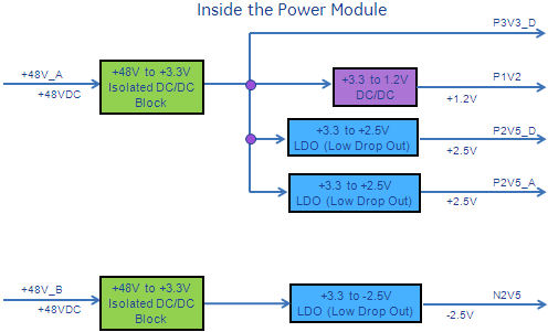
Power module generates several power sources for AD modules. There are two modules that has different part number but their difference is bracket only. Then PWA without the bracket is common and it will be FRU. Refer to Sec. 4 Power line for details.
3.3 SDCB External Interface
The following signals are removed. (no longer used).
-
Generator Interface (kV/mA feedback)
-
Detector FET Control Interface
With SDCB DAS, the kv/mA feedback signals are sent from ORP (SCORP) via RCIB CAN Bus communication.
4 Power Line
Figure 4. Power Line Wiring Diagram
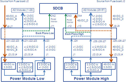
DAS Back plane receives 48VDC power from Fuse Board, and is sent to each Power module. Then Power module generates all of the power required to AD modules and send back to Back plane. The initial 3.3VDC DC/DC converter becomes the source of other voltage generator. That means if this 3.3VDC generator has an issue, then all of the power will be down. And they are provided to each AD module via Back plane. In Power Modules, 2.5VDC generator is separated for Analog use and Digital use (there are two generator modules). The power for SDCB (48VDC) is provided via Back Plane High. Back plane is exactly the board that has only connectors. For detail connection matrix, refer to BP Power Line matrix.
Figure 5. Power Module Block Diagram
5 Software Strings (DAS Type)
The following shows the comparison of DAS Type used in check_config command.
-
HDAS-Saturn_64 w/ DCB -> 10HW33.8.H40_P2_HS64_G_GMV --> DAS Type: HS64 (HALO-Saturn)
-
HDAS-Saturn_64 w/ SDCB -> 11HW34.16.H40_P2_SS64_G_GMV --> DAS Type: SS64 (SDCB-Saturn)