- Topic ID: id_11039053
- Version: 3.0
- Date: May 23, 2022 11:23:45 PM
DoD16 Pinouts, Jumpers and LEDs
1 External Interface Pinouts
For a full size of Illustration, click on the pdf icon below.
Figure 1. DoD57 Interface Pinout Block Diagram
5124748.pdfFigure 2. DoD57 Interface Pinout Block Diagram
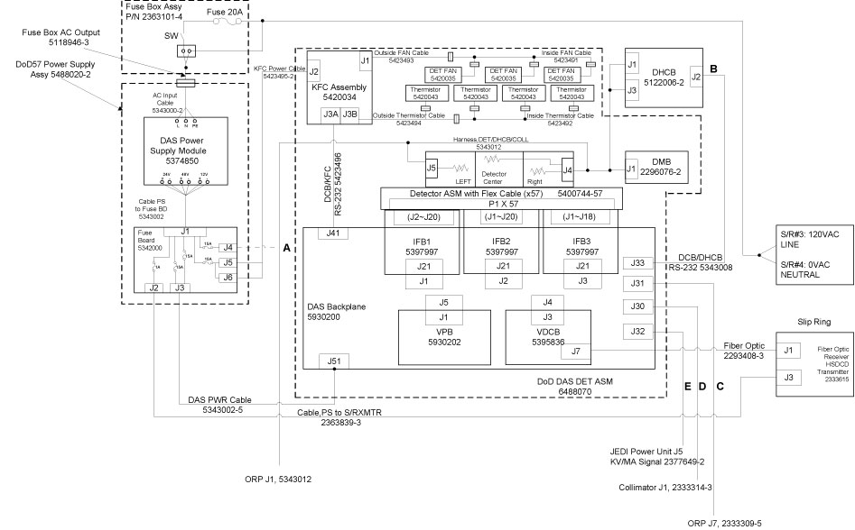
Letters next to Interconnect Cables represents further detailed descriptions in following pages.
1.1 Cable A: 5343012–3/5343012
DoD 24V DC power supply cable from fuse board (J4) to collimator, ORP and detector
1.2 Cable B: 5343008–2/5343008
Cable (RS-232) between DCB (J33) and DHCB (J2)
1.3 Cable C: 2333309–5
Analog Interface Cable from DAS Low Channel Backplane (J31) to ORP (J7).
1.4 Cable D: 2333314–3
DoD Data Cable from Collimator (J1) to DAS (J30).
1.5 Cable E: 2377649–2
kV/mA signal Cable, DAS (J32) to JEDI Power Unit (J5)
2 DIFB (DoD Interface Board)
Figure 3. DIFB
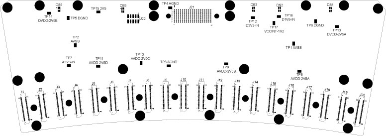
2.1 LEDs
The DIFB contains 5 LEDs to indicate the status of the IFB. These LEDs will be controlled by 5 FPGA separately.
A dual color (yellow + green) LED is provided on the DIFB to indicate the following information:
Yellow light indicated the trigger activity. Green light indicates the heartbeat of FPGA.
2.2 Test Points
Several test connectors shall be available for debugging purpose.
These are test points for 3.3V (analog input), 3.3V (digital input), 1.8V (digital input), 2.5V (analog for detector), 2.5V (digital for detector), 2.5V (digital for FPGA), 1.2V, analog ground and digital ground.
The DIFB provides the following test points:
2.3 Connectors
2.3.1 J1 to J20 (Detector Module) Overview
Connectors J1 to J20 are used to connect the detector module to the DIFB. Each connector can connect one detector module. This connector provides the interface for all digital signals to and from the detector module. Also provides connections for positive 2V5, 3V3 digital and 2V5, 3V3 analog. The connector is a 2 x 30 straight type connector.
The following is the pin assignment for J1 to J20:
2.3.2 J21 (Backplane) Overview
Connector J21 is used to connect the DIFB board to the backplane. This connector provides the interface for all digital signals to and from the DIFB board. Also provides connections for positive 1V8, 3V3 digital and analog 3V3. The connector is a 5 x 19 straight type connector with 2.0mm pitch. It also includes 2 extra lines for ground connections.
The following is the pin assignment for J21:
2.3.3 J22 (FPGA JTAG) Overview
Connector J22 is used to access the JTAG feature of the FPGA. This connector implements the JTAG interface to the Altera FPGAs. The connector is a standard male, straight 10-pin, 0.100”-spaced, straight header configuration.
The following is the pin assignment for J22:
3 DoD Control Board (DCB)
Figure 4. DCB
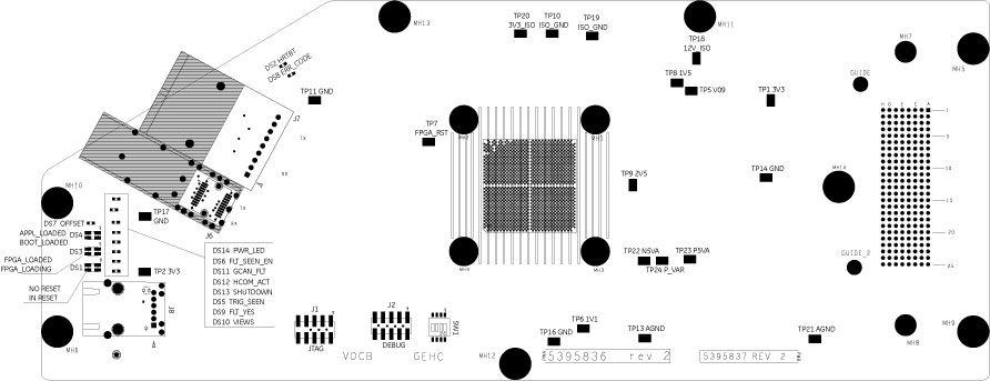
3.1 Board Layout
There are two connectors on the DoD DCB for normal operation:
A TX optical cable connector (J7) for high speed serial data transmission to the slip ring.
A backplane connector (J3) for below signals:
-
Power supply input: 3.3V, +12V and -12V from power board
-
Data, control and configruation signals from/to 3 pieces IFB boards
-
kV/mA signals from the Generator
-
RCIB signals from ORP and to CCB
-
Isolated RS232 signals to the Detector Heater Control Board (DHCB) and KunLun Fan Controller Board (KFC)
-
Debugging RS232 signals to backplane board connector (J52)
-
Two LED signals for BP’s LED (DCB_HEART LED, DCB_ERROR LED)
3.1.1 Pushbutton Reset
The pushbutton reset will initiate a hard reset to all the board logic. It will have the same effect as a reset initiated by the ORP. This initializes all the hardware to a known state, and causes the Nios processor to reboot.
3.1.2 Test Points
3.1.3 Switch
The DCB has a switch (SW1) which can be used to facilitate debugging in a lab environment.
The configuration for the switch are all OFF.
3.2 LEDs
The following table description the LEDs on the DCB.
3.3 Error Code
The DCB_ERROR LED flashes various patterns to indicate different error conditions. The DCB_ERROR indication is based on a two-digit system. To determine the first digit, the DCB will turn off the DCB_ERROR led for 2.5 seconds. It will then do an on-off pattern a certain number of times, with on and off times begin ~0.7seconds (~1.4sec total period). The number of times the on-off pattern occurs tells you the first digit. To determine the second digit, the DCB will turn off the DCB_ERROR led for 2.5 seconds. It will then do an on-off pattern a certain number of times, with on and off times begin ~0.25 seconds (~0.5sec total period). The number of times the on-off pattern occurs tells you the second digit.
The Error codes are defined as in below table.
3.4 DCB Backplane Connector Pinout
This section describes the DCB/BP connector pins assignment.
4 DoD Power Board (DPB)
Figure 5. DPB
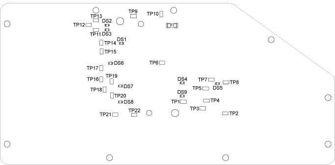
4.1 LEDs
4.2 Test Points
4.3 DPB Backplane Connector Pinout
Connector J1 is only connector of the DPB.
5 DoD Backplane (DBP)
5.1 LEDs
5.2 Test Points
Test Points are available on the Backplane to measure Power Supply voltages.
5.3 Connectors
5.3.1 External Interface
Power Input Connector (J51)
Connector J51 is 48V input interface for whole DAS system, the maximal current is less than 5A, the DBP transmits this power to DPB.
JEDI Connector (J32)
Connector J32 transmits kV and mA analog voltage from JEDI to DAS.
DHCB Connector (J33)
Connector J33 connects DHCB to DAS.
CFC Connector (J41)
Connector J41 connects the CFC board to DAS.
RCIB Connectors (J30, J31)
Connector J30 and J31 connect DAS with other subsystem such as collimator and ORP.
-
J30: RCIB_OUT
-
J31: RCIB_IN