- Topic ID: id_11039052
- Version: 3.0
- Date: May 23, 2022 11:23:43 PM
DoD16 (DAS on Detector) Theory
1 Overview
The purpose of the DAS is to accumulate snapshots (called views) of the x-ray image of the target, and move those snapshots through a high-speed link to the Host for processing. Each view is started by a trigger, which can be generated externally or internally (by a timer on the DCB).
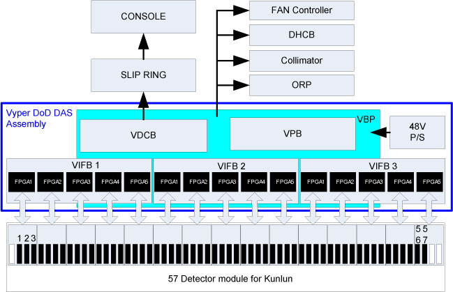
DoD16 DAS consists of 3pcs IFB, 1pcs DCB, 1pcs Power Board, 1 pcs Backplane, 1 pcs Power Source.
The purpose of the DCB firmware is to set up and control the hardware needed to acquire views and transmit them to the Host.
The hardware consists of the FPGA components on the DCB and the IFBs. The DCB can send requests to the IFBs to control them, or to query them for their status and/or settings.
It should be noted that the view data is not directly managed by the DCB firmware. The DCB FPGA is responsible for view acquisition from the IFBs and detector, and transmission to the host. The DCB’s firmware provides control information for the DCB FPGA to properly manage the data flow through the DAS and onto the Host.
The DCB itself is controlled via requests from the Host. Among the most important of the requests is the scan Rx, which, as the name implies, is the prescription for the scan. It provides the parameters needed to control the scan, including such information as the trigger frequency, the number of views to acquire, the starting view angle, and so on. Beyond the scan Rx, many other communications also come from the host, including status queries.
Figure 1. Vyper DoD16 DAS Block Diagram
DoD16 is comprised of the following components:
-
Detector and DAS Interface
-
The DIFB shall function as an interface bridge between the Detector Modules and the DAS control board (DCB).
-
The DPB provides the 3.3V and +/-12V power to DCB and provides the analog 3.3V, digital 3.3, and digital 1.8V power to three DIFBs.
-
The DAS Backplane is comprised of 1 boards that contain passive components only. The DBP is for communication of DAS and Detector.
-
The 48V power supply is a single power supply on the rotating assembly that powers most all of the components. This supply is not specific to the DAS. All voltages used by the DAS and Detector are generated via on board regulators on the DCB and DIFB's.
2 Detector and DAS Interface
Compared with original product based on Watson detector, interconnection between DoD16 detector and DAS is changed from signal to digital signal. In this case, DAS and detector interface is simplified accordingly.
DoD16 detector has total 57 detector modules and total 912 channels in x direction. On each module, there’re two kind of communication between DAS and detector in DoD16 design: single-end command for Vyper ASIC control and 12C communication for thermal sensor and EEPROM.
Figure 2. Detector Modules
2.1 Detector Module’s Vyper ASIC Interface Overview
The Vyper ASIC interface consist of: (Here, the “*” can be 1 to 20 and means detector module 1 to 20.)
-
four serial clocks (DM*_CLK01; DM*_CLK23; DM*_CLK45; DM*_CLK67)
-
eight serial data (DM*_D0_0; DM*_D0_1; DM*_D0_2; DM*_D0_3; DM*_D0_4; DM*_D0_5; DM*_D0_6; DM*_D0_7)
-
two chip selection (DM*_NCS0123; DM*_NCS4567)
-
two triggers (DM*_TRIG0123; DM*_TRIG4567)
-
two trigger enable (DM*_TRIGEN0123; DM*_TRIGEN4567)
-
two reset (DM*_RST1; DM*_RST2) line
Serial data port is customized I/O and other ports are output.
Serial clock, data and chip selection will work together for reading and writing the register of Vyper ASIC. Trigger and trigger enable will control the ASIC to sample input and AD conversion.
The interface can control 6 Vyper ASIC. Each ASIC has a serial data, two ASIC share one serial clock and four ASIC use one chip selection, trigger and trigger enable.
DIFB will configure the Detector module before scan through this interface, and then send triggers to control the ASIC conversion. Serial data link is also used to read back the conversion result when continuous conversion.
2.2 Detector Module’s I2C Interface Overview
I2C serial interface consist of a serial clock (SCL), serial data (SDA) and write protect (WP) line.
The I2C interface is used to access the Detector module’s memory and thermal sensor reading and writing. The detector module has two thermal sensor and one memory chip. These chip share one I2C interface and differentiated by address bits “A2 A1 A0”.
The memory and sensors have a unique 7-bit address allowing the master (FPGA) to access the I2C device. For the memory, the 7-bit address is “1 0 1 0 A2 A1 A0”. For the temperature sensor, the 7-bit address is “1 0 0 1 A2 A1 A0”. For Detector module design, A2, A1 and A0 equal logic 0 or ground.
The memory is 64Kbits FRAM and stores some detector module board information such as part number, version …etc. After DIFB is configured by DCB, DCB can read the data out from this memory by sending commons to DIFB.
The detector module has two thermal sensors. Each sensor will be read by DIFB’s FPGA controlling every 1s. The FPGA automatically reads the sensor via the I2C interface and saves the value in the 16bits width RAM.
3 DoD Control Board
The Vyper DoD DAS Control Board (DCB) is the main control board for the DoD slice Data Acquisition System (DAS). At a very high level, it controls the DAS and coordinates scans based on commands it gets from the On-board Rotating Processor (ORP).
3.1 Inputs
From Interface Boards (DIFB): Serial Data Streams
From On-Rotating Processor (ORP):
-
Input View Triggers
-
RCIB CAN Bus communication for scan prescription information and FLASH download
-
RCIB CAN Fault Signal
-
EXP CMD
-
CAN Reset
From Detector Heater Control Board (DHCB): RS-232 Bus communication for status, faults, detector temperature readings, and detector identification information
From Generator: kV & mA analog signals
From Backplane: Power supply voltages
3.2 Output
To Interface Boards:
-
Shift clock
-
Trigger signal
-
Reset signal
To On-Rotating Processor (ORP):
-
RCIB CAN Bus communication for DAS status, error, or scan complete information
-
RCIB CAN Fault Signal
To Detector Heater Control Board (DHCB): RS-232 Bus communication for control information
To Kunlun Fan Controller (KFC): RS-232 Bus communication for control information
To Slip-ring: High-speed serial data stream containing the view data with embedded FEC CRC.
3.3 Processing
The DCB performs the following functions:
-
Interfaces with the On-board Rotating Processor (ORP) for Rx reception and scan completion via CAN bus. Sets up gain and offset trim and controls the interface boards, via the DIFB data link.
-
Receives triggers and starts acquisitions with the interface cards.
-
The DAS shall be capable of supporting a range of discrete view (trigger) frequencies from 550 to 3936 Hz nominal trigger. 16-slice scanning.
-
Controls the operation of the Detector Heat Control Board (DHCB) and monitors the subsystem for faults.
-
Monitors the power supply voltages to make sure they are within the power supply limit.
-
Acquires the kV and mA values for each scan.
-
Have the capability to download the DCB image code into its flash memory, it include firmware/FPGA application code.
-
Have the capability to provide DCB part name/ID/Assembly revision/MFG related information, and Firmware version information.
-
Detects jitter and time-outs in the view trigger signal.
-
Stores & sums the z-axis reference channels, and performs calculations that control the collimator cam positioning. This is used to track the x-ray beam and keep it centered on the detector.
-
The DCB shall report error messages of VCS module/VIFB/VDCB/ORP to the system error log.
-
Monitors DAS temperature via KunLun Fan Controller Board (KFCB).
3.4 Control Signals
Two broadcast signals from the DCB are used to control the sequencing of data onto the data streams.
The trigger signal will be used to initiate the sampling and transmission of all the channels on the DIFB.
In response to an external or internal view trigger, DCB will generate a trigger pulse to all of the interface boards through the chassis backplane. Both external and internal view triggers have the same effect on the DCB.
The only mechanism to reset the converter boards will be to assert the reset signal. This active high, single-ended signal is set by the DCB and sent to all interface boards through the chassis backplane.
3.5 LS Signals In/Out
The LS used between the DCB and the DIFB is a bi-directional serial communications bus which is a LVDS signal. Communication is accomplished through a command/acknowledge protocol, rather than a register-access protocol.
3.6 HS Signals In
The DCB will accept DAS channel data from the DIFB, per the following definition. The Interface Board processes digital channel data from the ASIC’s resident on the VCS modules. This data is combined with temperature measurements into a single point-to-point serial data stream to the DCB.
3.7 Slipring Interface
The interface from the DCB to the console is designed to run at 833Mbaud per link, where each link represents a physical channel on the slipring.
3.8 Host CAN Interface
The DCB Host Interface will be used to control DAS operation and to communicate DAS status. The following sections describe the control interface. The DCB Host Interface makes use of Controller Area Network (CAN) technology. The DCB’s use of this technology including the physical interface conforms to all CAN specifications. All CAN signals are optically isolated between the DCB and the network.
The DCB receives the external view trigger input from the ORP via a twisted pair wire. This input signal is optically isolated from the DAS and causes the DAS to begin view data collection.
3.9 Generator Interface
kV and mA signals come from the X-ray generation subsystem and feed back to the DAS so they can be inserted into the view data stream. The Generator Interface is implemented on a connector located on the backplane and signals are routed to the DCB via the backplane. These signals are differentially driven by X-ray Generation and received by the DCB.
3.10 Detector Heater Control Board Interface
The DCB communicates with the Detector Heater Control Board (DHCB) using an RS-232 serial communication interface. This interface provides the path for the DCB to setup and control DHCB operation, to monitor the DHCB subsystem for faults, and to obtain detector temperature readings for inclusion in the view data stream.
On power-up the DCB detects the presence of the DHCB in the system. If the presence of the DHCB is detected, the DCB will begin to communicate with the DHCB via the RS-232 interface.
3.11 View Format
The detail view data format for DoD16 DAS is defined as below, all of them occupy two bytes for each channel. Cells in grey are invalid for the DoD49, but they are valid in DoD57.
4 DoD Interface Board
4.1 General
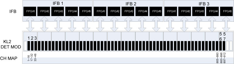
There will be 3 DoD16 DIFB boards in one chassis. One DoD16 DIFB will be mapped to 20 Detector Modules.
The DIFB reads ASIC channel data from multiple Detector Modules simultaneously and processes the data, and sends high-speed data to DCB in a serial stream.
All DIFB and DCB boards communicate with each other through the High speed serial interface.
4.2 Processing
The DIFB performs the following functions:
-
Voltage Regulation
-
Power Supply Sensing
-
Voltage Monitoring
-
Temperature Monitoring
-
Data Formatting (FFP)
-
Serial Interface with the Detector Module
-
ASIC on Detector Module Control
-
Point-To-Point Data Transmission to DCB
-
Linearization
-
Alpha Calibration
-
Trim Calculation
-
Thermal Calibration-Gain Tracking
-
Diagnostics
4.3 Interface Requirements
The DIFB board includes the following interfaces:
-
DCB to DIFB serial interface
-
DCB to DIFB configuration interface
-
JTAG interface
-
Detector module’s VYPER ASIC Serial Interface
-
Detector module’s I2C Interface
-
ADC I2C Interface
-
Analog To Digital Voltage Monitoring interface
5 DoD Power Board
5.1 General
Figure 3. DoD Power Board Block Diagram
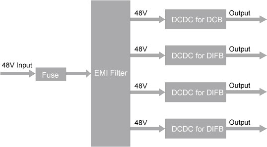
The DPB provides the following two functions:
-
Provide 3.3V and +/-12V power to DCB
-
Provide the analog 3.3V, digital 3.3V and digital 1.8V power to three DIFBs
5.2 Power Requirement
5.2.1 Power Requirement for DCB
DCB needs digital 3.3V 4A, ripple less than 100mV
DCB needs analog +/-12V 200mA, ripple less than 100mV
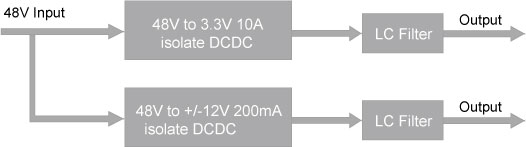
Figure 4. Power Block for DCB
5.2.2 Power Requirement for DIFB
The DPB provides three type powers to each DIFB.
-
Analog 3.3V 6A, ripple less than 100mV
-
Digital 3.3V 3A, ripple less than 100mV
-
Digital 1.8V 1.5A, ripple less than 100mV
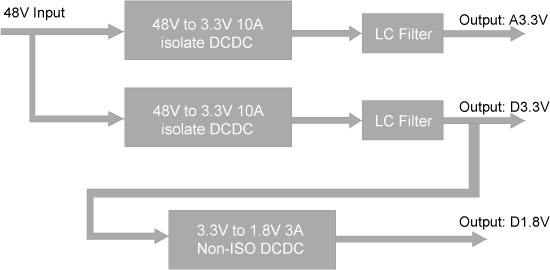
Figure 5. Power Block for DIFB
6 DoD Backplane
The DBP board includes the following functions:
-
Connect the three DIFBs, one DCB and one DPB in the Vyper DoD16 DAS system.
-
Provide the connection between inside and outside of DAS system, such as power input, JEDI, DHCB and RCIB interface.
-
Provide two LEDs to indicate the DCB heartbeat and report error.
Figure 6. DBP Connection Function Inside DAS System
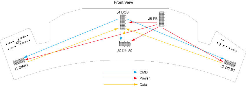
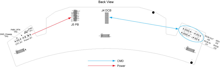
Figure 7. DBP Connection Function Between Inside and Outside DAS System
7 Power Supply
7.1 DAS Power Supply
The DAS power supply can ouput 48V, 24V and 12V voltage. It’s used to power the DAS, Detector subsystem, Collimator, ORP, Detector Heater Control Board, Fan Controller Board (KFC) and Slip ring Transmitter. All voltages used by the DAS and Detector are generated via on isolated DC-DC converter on power board. The power is supplied by regulators on the DIFB's. Each DIFB can power on up to 20 detector modules. There are no voltage adjustments for the DAS components. The Power supply has an internal fan for cooling.
The architecture of power supply is as below:
Figure 8. DoD16 DAS Power Supply Architecture
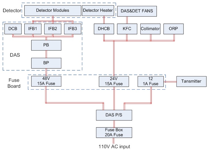
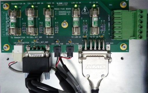
7.2 Fuse Board
The Fuse Board provides a central point for fuse protection and distribution of 48VDC power to the rotating harnesses and loads on the gantry. The board is powered by the main rotating 48VDC power supply. The loads served by this board are: DAS, Collimator, DHCB, KFC, ORP & Slip-Ring Transmitter.
Figure 9. DoD16 DAS Power Supply Fuse Board