- Topic ID: id_16157907
- Version: 1.0
- Date: Jul 7, 2018 4:28:35 PM
DCB Jumpers, LEDs, and Test Points
1 Board Layout
1.1 Overview
There are three connectors on the MDAS 16 DCB for normal operation: A TX optical cable connector for high speed serial data transmission to the slip ring, a RX optical cable connector for external loop-back testing, and a backplane connector for data and control signals to/from the Converter cards, signals from the Generator, RS232 interface to the Detector Heater Control Board (DHCB).
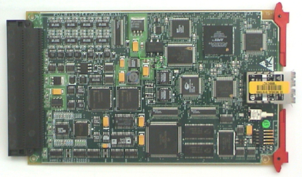
Figure 1. DAS Control Board Layout
1.2 Pushbutton Reset
The push-button reset, S1, initiates a hard reset to all the board logic. This initializes all the hardware to a known state, and causes the Core 68332 processor to reboot. The single FPGA, however, is only reconfigured from serial EEPROM at board power-up.
1.3 Test Points
The DCB Has the following test points:
-
TP1: JTAG Data Output for FPGA Programming
-
TP2: Digital Ground
-
TP3: +5V Digital Power
1.4 Jumpers
The DCB will have a single jumper in a straight, 2-pin male, 0.1-inch spacing, header-type connector. The factory configuration for the jumper is OUT. The jumper will be located on the DCB and will be accessible only when the DCB is out of the DAS chassis or the right chassis end plate is off. The pinout for the jumper block is shown in Table 2.
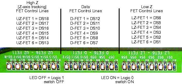
2 LEDs
Figure 2. DAS Control Board Layout - Reverse side, showing LEDs (at right)
Figure 3. Pulse Sequence Example