- Topic ID: id_16157995
- Version: 3.0
- Date: Nov 27, 2020 2:11:29 AM
Pancake DAS 16 Pinouts, Jumpers, and LEDs
1 External Interface Pinouts
Figure 1. PDAS 16 Interface Pinout Block Diagram
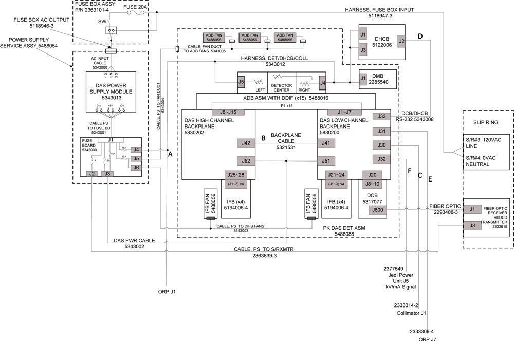
Letters next to Interconnect Cables represents further detailed descriptions in following pages.
1.1 Cable A
PDAS 24V DC power supply cable from fuse board (J4) to collimator, ORP and detector
1.2 Cable B
PDAS 16 Data Cable between Low Channel Backplane (J41) and High Channel Backplane (J42), J41 and J42 are of same pinout.
1.3 Cable C
PDAS 16 Data Cable from Collimator (J1) to DAS (J30).
1.4 Cable D
PDAS 16 Cable (RS-232) between DCB (J33) and DHCB (J2)
1.5 Cable E
Analog Interface Cable from DAS Low Channel Backplane (J31) to ORP (J7).
1.6 Cable F-2333310–2
PDAS 16 kV/mA signal Cable, DAS (J32) to JEDI Power Unit (J2)
2 ADB Converter Board Backplane Connector
Figure 2. ADB-to-Backplane connection, ADB side.
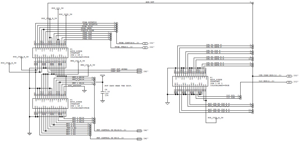
2.1 DDIF (DAS Detector InterFace)
There are eight DDIF connectors connected to 16 slice detector on ADB, M1~4A and M1~4B.
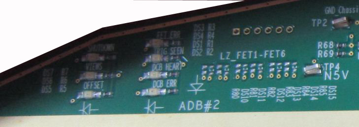
2.2 LEDs
Figure 3. ADB LEDs and Test Points
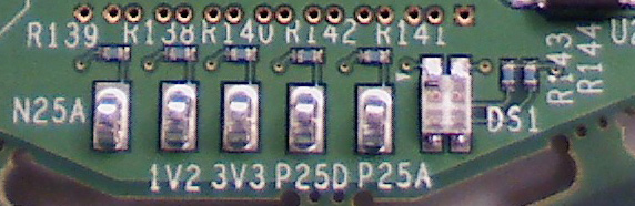
A dual color (orange + green) LED is provided on the ADB to indicate the following information:
2.3 Test Points
The ADB provides the following test points on Power and Ground:
3 PDAS Backplanes
3.1 LEDs
Figure 4. Backplane (5830200) LED's
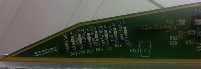
3.1.1
Figure 5. Backplane (5830200–2) LED's
3.2 Power Supply Test Points
Test Points are available on the Backplane to measure Power Supply voltages.
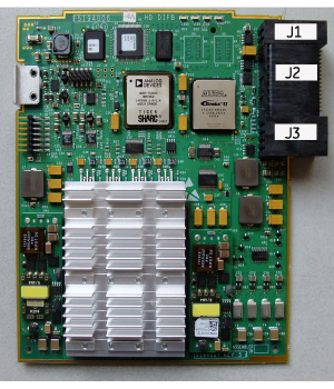
4 Digital InterFace Board (DIFB)
There are three connectors (J1, J2 and J3) on the PDAS 16 DIFB for normal operation. The three connectors are to connect the DIFB to the PDAS backplane.
-
J1: This connector is for getting power input from the PDAS backplane.
-
J2: This connector provides the interface for all digital signals to and from the DIFB board. It also provides connections for positive 2V5 and 3V3 digital and analog power supplies to ADB. The connector is a Tyco multigig 8 x 16 right angle type connector with 1.8mm pitch. It also includes 3 extra rows for ground connections.
-
J3: This connector supplies power to the ADB boards.
4.1 Board Layout
Figure 6. Digital InterFace Board Layout
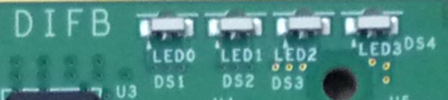
4.2 LEDs
Figure 7. DIFB LED's
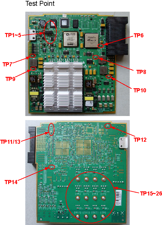
4.3 Test Points
Figure 8. DIFB Test Points
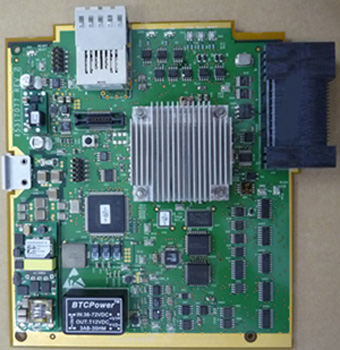
5 DAS Control Board (DCB)
5.1 Board Layout
There are three connectors on the PDAS 16 DCB for normal operation: A TX optical cable connector for high speed serial data transmission to the slip ring, a RX optical cable connector for external loopback testing, and a backplane connector for data and control signals to/from the Converter cards, signals from the Generator, RS232 interface to the Detector Heater Control Board (DHCB).
Figure 9. DAS Control Board Layout
5.1.1 Pushbutton Reset
The pushbutton reset will initiate a hard reset to all the board logic. It will have the same affect as a reset initiated by the ORP. This initializes all the hardware to a known state, and causes the Nios processor to reboot. This reset is provided for debug and bring-up purposes only, it will not be used in a production environment.
5.1.2 Test Points
The DCB Has the following test points as shown in below table:
5.1.3 Switch
The DCB has a Switch(SW1) which can be used to facilitate debugging in a lab environment. The factory configuration for the switch are all off. The Switch will be located on the DCB and will be accessible only when the DCB is out of the DAS. The description for the Switch is shown in Table 28.
5.2 LEDs
The following table describes the LED’s on the DCB.
5.3 Error Code
The ERR_CODE led flashes various patterns to indicate different error conditions. The ERR_CODE indication is based on a two-digit system. To determine the first digit, the DCB will turn off the ERR_CODE led for 2.5 seconds. It will then do an on-off pattern a certain number of times, with on and off times begin ~0.7seconds (~1.4sec total period). The number of times the on-off pattern occurs tells you the first digit. To determine the second digit, the DCB will turn off the ERR_CODE led for 2.5 seconds. It will then do an on-off pattern a certain number of times, with on and off times begin ~0.25 seconds (~0.5sec total period). The number of times the on-off pattern occurs tells you the second digit.
The Error codes are defined as in below table.
5.4 Detector Heater Control Board (DHCB)
5.5 DCB Backplane Connector Pinout
Figure 10. : DCB to BACKPLANE Connector
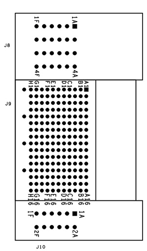
The following table shows all three DCB Multi-gig (J8, J9, J10) connectors, which produce the DCB to BACKPLANE connection. The top connector (J8) is a four positions’ power module. The middle connector (J9) is a 128 position Multi-gig connector. The bottom connector (J10) is a two position power module.