- Topic ID: id_16157707
- Version: 1.0
- Date: Jul 7, 2018 4:26:33 PM
MDAS 16 Pinouts, Jumpers, and LEDs
1 External Interface Pinouts
Figure 1. MDAS 16 Interface Pinout Block Diagram
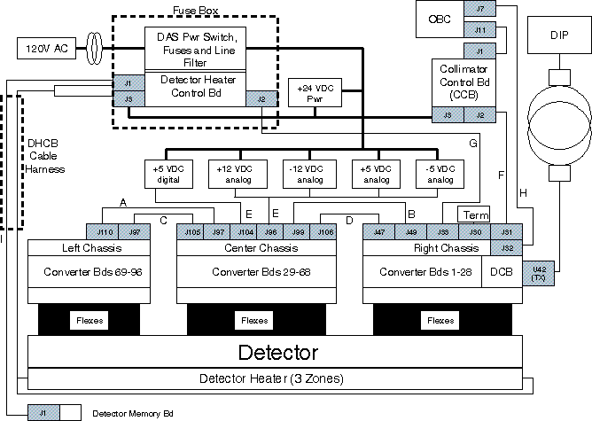
Letters next to Interconnect Cables represents further detailed descriptions in following pages.
1.1 Cable A
MDAS 16 Power Cable between Center (J97) and Left MDAS 16 Chassis (J110)
1.2 Cable B
MDAS 16 Power Cable between Center (J99) and Right MDAS 16 Chassis (J49)
1.3 Cables C & D
DAS Data Cables between Left DAS Chassis, Center DAS Chassis and Right DAS Chassis.
1.4 Cable E
MDAS 16 Power Harness from MDAS 16 Power Supplies to Center MDAS 16 Chassis (J96 & J104)
1.5 Cable F
MDAS 16 Cable from Collimator (J2) to DAS CAN (J31).
1.6 Cable G
MDAS 16 Cable (RS-232) between DCB (J33) and DHCB (J2)
1.7 Cable H
Analog Interface Cable from Right DAS Chassis (J32) to OBC (J7). The Analog Interface Cable is used for monitoring the KV & MA analog control voltages.
1.8 Cable I
MDAS 16 Cable, DET/DHCB (J1,J3)/DMB (J1)/Collimator (J3)
2 Converter Board Backplane Connector
The Converter Board uses a 192 (4 x 48) pin, right-angle gold-plated connector.
Figure 2. Converter board backplane connector (viewed with DAS at 12 o’clock)
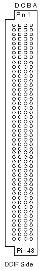
Pin assignments are shown in Table 9.
3 DAS Backplanes
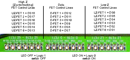
3.1 LEDs
MDAS 16 LEDs are located on the Right Backplane. Low Z FET lines are set the same as Data FET lines in the current implementation.
Figure 3. MDAS 16 LEDs (as viewed with DAS at 12 o’clock)
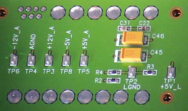
3.2 Power Supply Test Points
Test Points are available on the Center Backplane to measure Power Supply voltages.
Figure 4. MDAS 16 Center Chassis Power Supply Test Points
3.3 Detector Bias Test Points -5v_A (DVSS)
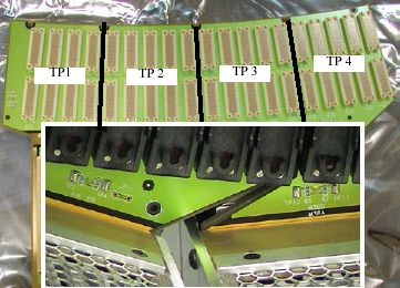
The MDAS16 backplanes have limiting resistors (392 ohms nominal) between the DVSS (-5V_A) supply and the Detector flex module connections. These resistors limit the current to prevent the backplane traces from fusing in the case of a short on the DDIF.
Each distinct backplane has been divided up into 4 groups of modules, each group having its own limiting resistor and test point. This is to make finding the shorted module easier. Each test point is referenced to the DAS center chassis TP 4 AGND test point.
Figure 5. Right Backplane DVSS (-5v_A) Zone Coverage
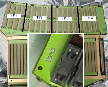
Figure 6. Center Backplane DVSS (-5v_A) Zone Coverage
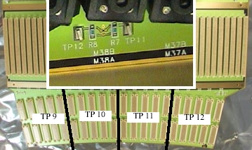
Figure 7. Left Backplane DVSS (-5v_A) Zone Coverage
4 DAS Control Board (DCB)
4.1 Board Layout
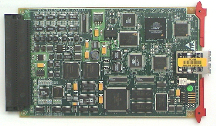
There are three connectors on the MDAS 16 DCB for normal operation: A TX optical cable connector for high speed serial data transmission to the slip ring, a RX optical cable connector for external loopback testing, and a backplane connector for data and control signals to/from the Converter cards, signals from the Generator, RS232 interface to the Detector Heater Control Board (DHCB).
Figure 8. DAS Control Board Layout
4.1.1 Pushbutton Reset
The pushbutton reset, S1, initiates a hard reset to all the board logic. This initializes all the hardware to a known state, and causes the Core 68332 processor to reboot. The single FPGA, however, is only reconfigured from serial EEPROM at board power-up.
4.1.2 Test Points
The DCB Has the following test points:
-
TP1: JTAG Data Output for FPGA Programming
-
TP2: Digital Ground
-
TP3: +5V Digital Power
4.1.3 Jumpers
The DCB will have a single jumper in a straight, 2-pin male, 0.1-inch spacing, header-type connector. The factory configuration for the jumper is OUT. The jumper will be located on the DCB and will be accessible only when the DCB is out of the DAS chassis or the right chassis end plate is off. The pinout for the jumper block is shown in Table 13.
4.2 LEDs
Figure 9. DAS Control Board Layout - Reverse side, showing LEDs (at right)
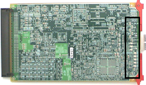
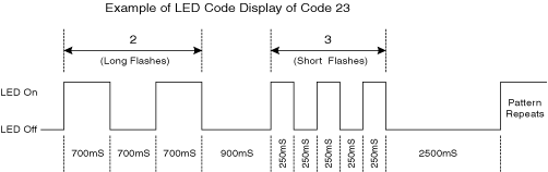
Figure 10. Pulse Sequence Example
4.3 Detector Heater Control Board (DHCB)
4.4 DCB Backplane Connector Pinout
Figure 11. DCB backplane connector (viewed with DAS at 12 o’clock)