- Topic ID: id_18718233
- Version: 1.0
- Date: Sep 20, 2018 2:02:14 PM
GDAS(4/8) Pinouts, Jumpers, and LEDs
1 External Interface Pinouts
Figure 1. GDAS 4-8 slice Interface Pinout Block Diagram
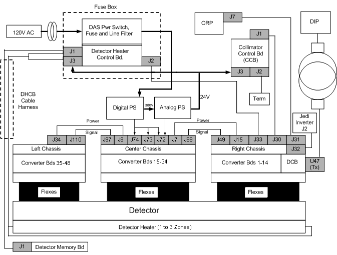
Letters next to Interconnect Cables represents further detailed descriptions in following sections.
1.1 Cable A
GDAS Power Cable between Center (J97) and Left GDAS Chassis (J110)
1.2 Cable B
GDAS Power Cable between Center (J99) and Right GDAS Chassis (J49)
1.3 Cables C
DAS Data Cables between Left DAS Chassis, Center DAS Chassis and Right DAS Chassis.
1.4 Cable E
GDAS Power Harness from GDAS Power Supplies to Center GDAS Chassis (J72, J73, & J74)
1.5 Cable F
GDAS Cable from ORP (J7) to DAS CAN (J31).
1.6 Cable G
GDAS Cable (RS-232) between DCB (J33) and DHCB (J2)
1.7 Cable H
Analog Interface Cable from Right DAS Chassis (J32) to JEDI Power Unit (J5). The Analog Interface Cable is used for monitoring the KV & MA analog control voltages.
1.8 Cable I
GDAS Cable, DET/DHCB (J1,J3)/DMB (J1)/Collimator (J3)
2 Converter Board Backplane Connector
The Converter Board uses a 192 (4 x 48) pin, right-angle gold-plated connector.
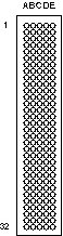
Figure 2. Converter board backplane connector (viewed with DAS at 12 o’clock)
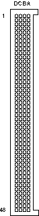
Pin assignments are shown in Table 9
3 DAS Backplanes
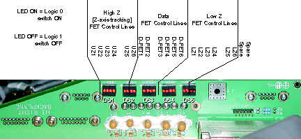
3.1 LEDs
GDAS LEDs are located on the Right Backplane.
Figure 3. GDAS LEDs (as viewed with DAS at 12 o’clock)
3.2 Power Supply Test Points
Test Points are available on the Center Backplane to measure Power Supply voltages.
4 DAS Control Board (DCB)
4.1 Board Layout
The GDAS DCB differs from the MDAS DCB physically in that it is packaged in the right DAS chassis with the Converter boards. This eliminates a number of cables and connectors. There are only two connectors on the DCB for normal operation: An optical cable connector for high speed serial data transmission to the slip ring and a backplane connector for data and control signals to/from the Converter cards, signals from the Generator, RS232 interface to the Detector Heater Control Board (DHCB).
Figure 4. DAS Control Board Layout
4.1.1 Pushbutton Reset
The pushbutton reset, S1, initiates a hard reset to all the board logic. This initializes all the hardware to a known state, and causes the Core 68332 processor to reboot. The FPGA, however, is only reconfigured from serial EEPROM at board power-up.
4.1.2 Test Points
The DCB Has the following test points:
-
TP1: +5V Digital Power
-
TP2: Digital Ground
4.1.3 Jumpers
The DCB has three jumpers of header-type connector. The factory configuration for each jumper is OUT. The normal Applications Mode is both jumpers OUT. These jumpers are located on the DCB and are accessible only when the DCB is out of the DAS chassis or the cover for the right chassis is off.
4.2 LEDs
Figure 5. DAS Control Board Layout - Reverse side, showing LEDs (at bottom)
4.3 Detector Heater Control Board (DHCB)
Reference “Detector Heater Control Board (DHCB),” in Warp3 Detector Theory.
4.4 Backplane Connector Pinout
Figure 6. DCB backplane connector (viewed with DAS at 12 o’clock)